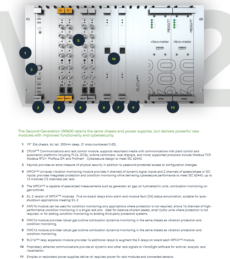
Meggitt VM600 MPS Mechanical Protection System
Meggitt VM600 MPS (Mechanical Protection System) is a modular digital protection system used for monitoring and protecting parameters such as vibration and temperature in industrial rotating machinery. It supports two types of racks, ABE04x (6U) and ABE056 (1U), and is equipped with MPC4/AMC8 core processing cards and IOC4T/IOC8T input/output cards. It has 4-8 measurement channels and 2 speed channels, supports voltage/current signal input, multiple signal processing modes, and alarm logic combinations. It is controlled by OC Bus/Raw Bus extension relays, compatible with RS-232/Ethernet communication, and meets industry standards such as API 670 and IEC 61508. It is suitable for compressors and gas turbines in the fields of power, oil and gas, etc. Waiting for device protection.
Core architecture and hardware composition of the product
1. Rack and power system
Rack model, size, specifications, compatibility, number of power card slots, core features
ABE04x (ABE040/ABE042) 19 “× 6U RPS6U (300W/330W) 21 VME slots (0-20) support redundant power supply and multi module expansion
ABE056 19 “× 1U RPS1U (AC/DC input) 3 VME slots (1, 3, x) slim line design, space saving
Key parameters of power module:
RPS6U: Output+5V (35A/50A), ± 12V, supports AC (115/230V) or DC (24/110V) input
Redundant configuration: Dual RPS6U can achieve power redundancy or power expansion, supporting hot swapping
2. Core functional modules
Module type represents model, core function, key specifications
Vibration protection card MPC4 vibration signal processing, speed monitoring with 4 measurement channels, 2 speed channels, SIL version optional
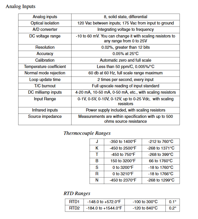
Simulate monitoring card AMC8 for quasi-static parameter monitoring such as temperature and pressure, with 8 measurement channels and support for thermocouple/RTD input
Control card CPUM rack control, network communication support Ethernet/RS-232, Modbus TCP
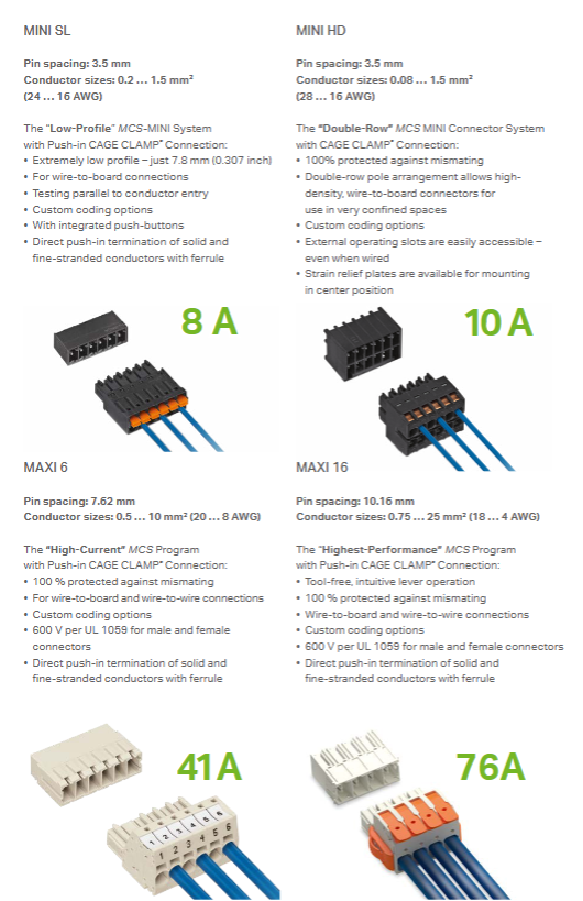
Input/output card IOC4T/IOC8T sensor wiring, signal conversion screw terminal (≤ 1.5mm ² wire diameter), DC output (4-20mA/0-10V)
Relay expansion card RLC16/IRC4 alarm output expansion RLC16 (16 channels), IRC4 (8 channels, supporting DSDT/SPDT)
Signal processing and measurement capabilities
1. Input signal type
Vibration signals: acceleration, velocity, displacement (supporting accelerometers, proximity probes, etc.)
Temperature signal: thermocouple (E/J/K/T type) RTD(Pt100/Cu10/Ni120)
Speed signal: magneto electric sensor, TTL signal (0.3Hz-50kHz)
Other signals: 4-20mA current signal, 0-10V voltage signal (pressure, flow rate, etc.)
2. Core processing mode
Vibration processing: broadband absolute vibration (BBAB), shaft relative vibration (RS), eccentricity (EC), Smax measurement
Temperature/pressure processing: quasi-static measurement, differential measurement, linear compensation
Speed processing: speed calculation, phase reference, trigger threshold adaptive
Rectification method: RMS, mean, peak, peak to peak (supports True Peak/Peak to Peak)
3. Alarm and control functions
Alarm level: Alert+/-, Danger+/- four level alarm
Alarm configuration: Delay (Δ t), hysteresis value, and latch function can be set
Logical combination: Supports 8 basic logics (AND/OR/voting logics) and 4 advanced logical combinations
Control functions: Danger Bypass, Trip Multiply, Channel Inhibit
Extended control: Drive external relays through OC Bus (16 channels) and Raw Bus (64 channels)

Communication and Interface
1. Communication method
Local communication: RS-232 (single card configuration)
Network communication: Ethernet (CPUM module) Modbus TCP/RTU
Bus support: VME bus (in rack module communication), Tacho Bus (speed signal sharing)
Expansion interface: RS-485 (supports half duplex/full duplex)
2. Signal interface specifications
Input terminals: screw terminals (IOC4T/IOC8T), BNC (MPC4 panel, RAW signal output)
Output signal: DC output (4-20mA or 0-10V), relay contact output
Shielding design: Sensor cable shielding grounding, supporting galvanic separation (GSI module)
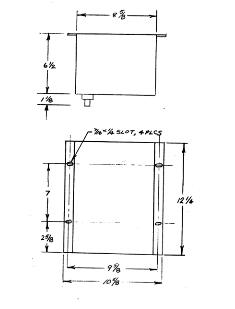
Installation and compliance requirements
1. Installation specifications
Ventilation requirements: Natural ventilation requires reserved spacing (ABE04x ≥ 50mm, ABE056 ≥ 20mm), and forced air cooling is recommended for high temperature environments
Grounding configuration: Rack grounding (PE), signal shielding grounding, supporting switching between VME grounding and chassis grounding
Hot swappable support: MPC4/AMC8 and other modules can be plugged and unplugged with power on, CPUM/RPS6U needs to be replaced with power off
2. Compliance and environmental adaptation
Industry standards: API 670 (Mechanical Protection), IEC 61508 (Functional Safety), IEC 62443 (Network Security)
Environmental parameters: operating temperature -20 ℃~60 ℃, storage temperature -40 ℃~85 ℃
Dangerous area: Class 2/Div 2 compatible, supports Class 1/Div 1 (with safety barrier)
5、 Maintenance and Support
Troubleshooting: Built in BITE (self check), LED status indicator, software diagnosis
Card replacement: Supports separate module replacement, configuration can be backed up/restored through software
Long term storage: The power module needs to be removed, and the storage environment should be dry and non corrosive
Service Support: Provide technical consultation, repair returns, document updates (downloadable from the official website)