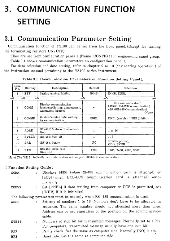
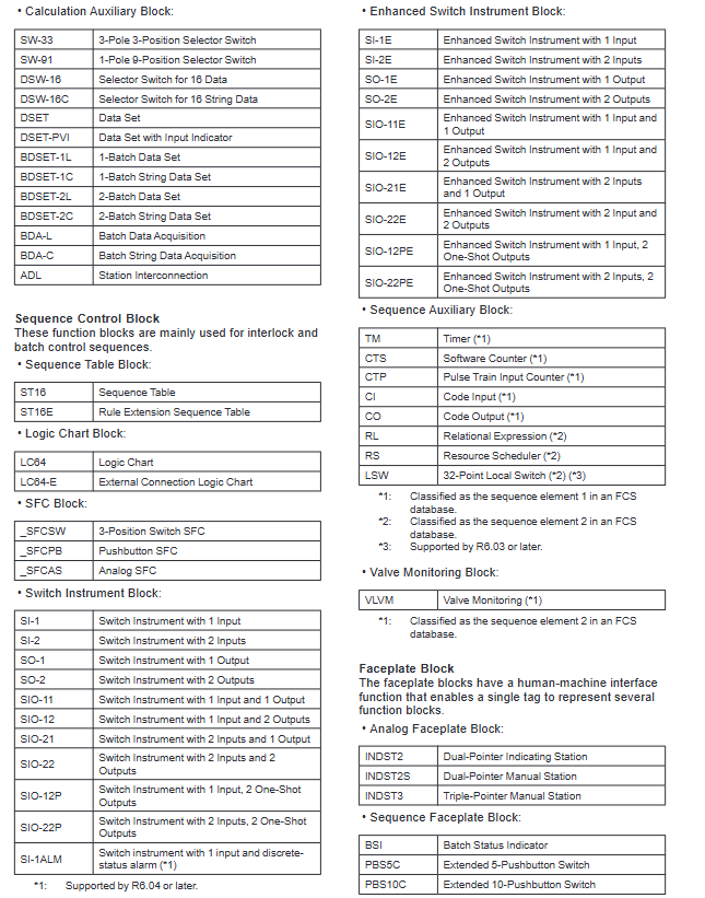
The YS100 series instruments (including YS150/YS170/YS131/YS135/YS136 models) support RS-485 (option code/A31) and DCS-LCS (option code/A32) communication functions. The former can be interconnected with multiple monitoring computers (up to 16 units, communication distance ≤ 1200m), while the latter can be connected to the Yokogawa CENTUM-XL/μ XL DCS system (up to 24 units/EFCS); The core communication parameters include baud rate of 1200-9600bps, half duplex mode, ASCII 8-bit encoding, support for data read and write (DG/DP commands), watchdog timer settings, and other functions. The parameters need to be configured through the front-end panel to adapt to the monitoring and operation requirements in industrial process control, while providing a comprehensive error handling mechanism and programming examples.
Core communication specifications
(1) RS-485 communication specifications
Category specific parameters
Communication interface RS-485 five signals: SD (A), SD (B), RD (A), RD (B), SG (signal ground)
Communication protocol without protocol (command response format), asynchronous operation
The core function of YS100 is registered as an internal instrument of DCS, which can be monitored, operated, and parameter set through the DCS operator station
Installation and parameter configuration
(1) Terminal allocation
Terminal number RS-485 communication function DCS-LCS communication function
PH1/PL1 high and low limit alarm set values for the entire series -6.3~106.3% can be written
PRCA process alarm status series 8-bit binary (0=normal/1=fault) read-only
LS1/LS2 operating modes YS150/YS170 MAN/OUT/CAS/SPC/DDC can be written
(3) DCS-LCS communication correspondence
YS100 DCS Instrument Model Core Monitored Parameters
YS150 SLPC PV, SV, MV, P (proportional band), I (integral time), D (derivative time)
YS170 SLPC PV、SV、MV、 Program control parameters, alarm status
YS135 SMST-111 PV、SV、 High and low limit alarm setting values
YS136 SMST-121 PV、MV、 Upper and lower limits of manipulated variables
Error Handling and Programming Examples
(1) Common types of errors and their handling
Measures for handling error type phenomena
Communication parameters do not match, instrument does not respond, unified computer and instrument baud rate, parity check and other parameters
Address error: The instrument is unresponsive. Please confirm the instrument address (1-16) to avoid duplicate allocation
The response message is too long and returns an error code @ 100. Reduce the amount of data read in a single attempt and ensure that the message is ≤ 220 bytes
Return the corresponding error code for syntax errors (such as @ 011=invalid command). Check the command format, parameter names, and data format
(2) Programming Example
Provide an IBM-PC BASIC program example for reading data from YS100 instrument PV1, SV1, and MV1 at address 01. The core steps include port configuration, command sending, response receiving, and display.
User Program Example (YS170 Proportional Controller)
Proportional control is achieved through DCS-LCS communication, using BS (corresponding to P1 parameter) to set the proportional coefficient, X2 as the cascaded input value, Y4/Y5 as the communication register feedback intermediate calculation result, and finally outputting CSV1 as the set value to drive the control loop.
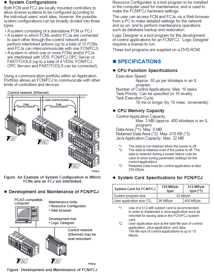
FCN/FCJ are two core autonomous controllers under Yokogawa Electric Corporation’s STARDOM series, designed specifically for industrial automation scenarios. They are suitable for various industrial processes from sequence control to analog control, and can achieve core functions such as equipment linkage, parameter adjustment, data acquisition, and monitoring. The two products are designed with modularity (FCN) and integration (FCJ) respectively, adapting to different installation environments and system complexity requirements. They are widely used in distributed control systems in factories, built-in control of mechanical equipment, industrial process monitoring and other scenarios, providing highly reliable and efficient control solutions for industrial production.
(2) Product Classification and Definition
Product type, English abbreviation, meaning, structural characteristics, subdivision models, and core configurations
FCN Field Control Node has a modular structure that can be flexibly matched with CPU, I/O, and other expansion modules according to needs, with strong scalability – FCN-100: equipped with NFCP100 CPU module
-FCN-500: Equipped with NFCP501/NFCP502 CPU modules
-FCN-RTU: equipped with NFCP050 CPU module, low-power design
FCJ Field Control Junction integrated structure, built-in I/O interface, no need for additional module assembly, compact structure without subdivision models, unified as FCJ series, integrated control and I/O functions
Core product features
(1) High performance: adaptable to diverse control requirements
Multi process compatibility: It can seamlessly integrate various industrial processes such as sequence control and analog control, and can meet the control needs of different processes without the need to replace controllers, reducing system upgrade and maintenance costs.
Flexible operation mode: supports independent operation (single controller completes local control) and interconnected control (communicates and links with other autonomous controllers or external devices), adapting to system architectures ranging from simple to complex.
Software linkage extension:
Paired with Versatile Data Server (VDS) or Supervisory Systems (FAST/TOOLS), a feature rich operation and monitoring system can be built to achieve advanced functions such as centralized data management, visual monitoring, and report generation.
Supports FCN/FCJ OPC servers, and PC OPC clients (following the OLE for Process Control standard) can directly access controller data, achieving cross platform data interaction.
Java Scalability: Built in Java Virtual Machine, supporting various Java application development and deployment, including:
Web browser image display: Visualize device status, control parameters, and other information through web pages.
Data management: Save data files locally and transfer files through FTP protocol.
Communication extension: Sending/receiving emails (supporting SMTP/POP3 protocol and SMTP server authentication), connecting to the public network through PPP protocol (such as GPRS network).
Programming free application: Paired with InfoWell software, web browsing, email communication, and other functions can be achieved without writing code, reducing the threshold for application deployment.
(2) High reliability: ensuring continuous operation of industry
Comprehensive diagnosis and protection: Equipped with complete RAS features (CPU self diagnosis, temperature monitoring, I/O diagnosis, etc.), it can monitor the equipment’s operating status in real time, detect faults in a timely manner, and issue alarms; Equipped with ECC (Error Correcting Code) error correction memory, effectively avoiding control exceptions caused by memory data errors.
Low power fanless design: High heat dissipation efficiency, stable operation without the need for a cooling fan, reducing mechanical failure points, suitable for harsh environments with high dust and vibration in industrial sites.
Dual redundant configuration:
FCN-100: The Ethernet control network, CPU module, power module, and SB bus (local bus) can all be configured with dual redundancy, allowing seamless switching in case of any component failure without downtime.
FCJ: The control network supports dual redundancy to ensure the continuity of communication links and meet the high reliability communication requirements of distributed systems.
(3) Engineering Efficiency: Simplify Development and Configuration
Multi programming language support: compatible with 5 IEC 61131-3 standard programming languages (such as ladder diagrams, functional block diagrams, instruction lists, etc.), users can flexibly choose according to process requirements and development habits, reducing programming barriers.
Software component reuse: Control logic can be encapsulated as standardized software components, supporting reuse, avoiding duplicate development, improving system configuration efficiency and consistency, and ensuring control quality.
Application Portfolios: Built in Yokogawa Electric’s years of industrial application experience, providing rich pre made software packages that can quickly implement advanced functions, including:
Control class: Control circuit instrument blocks (such as PID controllers, indicators, etc.).
Communication class: Communication adaptation module for non Yokogawa PLCs (such as Mitsubishi MELSEC, Omron SYSMAC, etc.).
(4) Maintainability: Reduce operation and maintenance costs
Online download function: During system operation, control applications can be directly modified, supporting the addition, deletion, and modification of I/O interfaces, variables, data types, program code, and library files. Modifying a single control circuit does not affect the operation of other circuits, and does not require shutdown maintenance, ensuring production continuity.
Hot swappable support: All modules of FCN-100 support hot swappable, so there is no need to cut off the system power when replacing faulty modules, further reducing downtime.
Convenient maintenance tool: supports remote access to the controller through a web browser for network configuration, database backup/recovery, parameter adjustment, and other maintenance operations; Paired with the Resource Configurator tool, hardware parameter configuration can be quickly completed, improving operational efficiency.
System configuration and development maintenance
(1) System configuration type
FCN/FCJ are both locally installed controllers that can be flexibly configured with three system architectures according to user on-site needs:
Independent system: A single FCN or FCJ operates independently, suitable for local area control (such as a single device or production unit), with a simple structure and low deployment cost.
Interconnected system: Multiple FCNs/FCJs are interconnected through a control network to achieve cross device linkage control. It supports communication between up to 15 FCNs/FCJs and one controller, adapting to distributed production scenarios such as multi workshop and multi production line collaboration.
Linkage system: One or more FCN/FCJ are linked with upper level software such as VDS, FCN/FCJ OPC Server, FAST/TOOLS, etc., supporting up to four such software to connect simultaneously, achieving centralized monitoring and advanced data management.
Cross device communication: Through the communication module in the application package, it can be interconnected with third-party controllers, display units, temperature controllers, power monitoring devices, and other devices to expand system compatibility.
(2) Development and maintenance tools
Tool Name Core Function Operation Requirements
Logic Designer develops FCN/FCJ control applications (organized in task form), supports IEC 61131-3 standard programming language, requires separate license purchase, runs on PC/AT compatible machines
The Resource Configurator is used to configure the hardware parameters of the controller, including IP address, I/O module model, license activation, initial communication protocol settings, etc. No license is required, and it is provided free of charge with the software DVD-ROM
Web browser remote access controller for network configuration, database backup/recovery, device status monitoring and other maintenance operations. Supports mainstream browsers and connects to the controller via Ethernet
FCN/FCJ Simulator simulates the controller operating environment on a general-purpose PC and debugs control applications developed by Logic Designer without the need for actual controller hardware. A separate license needs to be purchased and is provided with the software DVD-ROM
(3) Development and maintenance process
Hardware configuration: Set basic parameters such as controller IP address, I/O module model, communication protocol, etc. through the Resource Configurator tool.
Application development: Use Logic Designer to write control programs (tasks), support multi task parallel design, and specify task priorities and execution cycles.
Debugging and testing: Use FCN/FCJ Simulator to debug the program on the PC side and verify the correctness of the control logic; After debugging, download it to the controller via Ethernet.
Operation and maintenance: During the operation of the system, the device status is monitored through a web browser or local tools. If program modifications are needed, they can be updated through the online download function. In case of faults, modules can be hot plugged and replaced.
Key technical specifications
(1) CPU function and memory specifications
CPU core parameters:
Execution speed: The instruction list (IL) program has a processing speed of about 50 µ s/thousand steps, with high computational efficiency, which can meet the real-time control requirements of industry.
Control application capacity: Supports up to 16 tasks, with task priorities divided into 16 levels and execution cycles ≥ 10 ms (adjusted in increments of 10 ms), suitable for multi task parallel control scenarios.
Memory capacity allocation:
Control application capacity: up to 3 MB, capable of storing approximately 400 thousand steps of IL program.
Data area: Maximum 8 MB, used to store temporary data during runtime, not retained after power failure.
Reserved data area: up to 410 KB (including 350 KB dedicated to control applications), data will not be lost after power failure, and key information such as control parameters and tuning settings can be stored.
Java application capacity: up to 32 MB, used for deploying Java applications.
(2) System card specifications
The system card is used to store system programs, user applications (control programs+Java programs), and data, and offers two specifications to choose from:
System card type, system program occupying space, user application total capacity, recommended usage scenarios
128 MB type 32 MB 96 MB (control application ≤ 10 MB) No complex Java applications, only running basic control programs
512 MB type 32 MB 480 MB (control application ≤ 10 MB) requires running Java applications such as InfoWell, or storing a large amount of historical data
(3) Network communication specifications
1. Ethernet (Control Network)
Standard compatibility: Following the IEEE802.3 standard, supporting dual redundancy configuration to ensure communication reliability.
Core purpose: To connect FCN/FCJ, PLC, display unit, VDS and other devices, and also for the development and maintenance of controllers (program download, parameter configuration).
Connection ability:
Remarks on the maximum number of connections for the connection target
VDS/FCN/FCJ OPC Server/FAST/TOOLS 4 units, total number of Class III devices not exceeding 4 units
FCN/FCJ controllers can link up to 15 devices of the same type with a single controller
32 third-party PLCs (such as FA-M3, MELSEC), each occupying 1 communication channel
2. Serial communication
Purpose: To connect display units, temperature controllers, power monitors, and other devices, supporting multiple serial communication protocols.
Hardware configuration:
Controller type serial port configuration remarks
FCJ 2 RS-232-C ports fixed configuration, non expandable
The FCN-100 CPU module comes with one RS-232-C port; Expandable serial communication module (2 ports per module, supporting RS-232-C or RS-422/RS-485) can install up to 8 expansion modules, and the CPU’s built-in serial port is not available when using dual redundant CPUs
(4) Control the upper limit of application capacity
Function Blocks (POUs): Supports up to 512, including:
Regulator control blocks (such as indicators, controllers, manual loaders): ≤ 128.
Other functional blocks (such as calculation block, switch instrument block, communication POU): ≤ 384.
I/O interface: 96 AI (analog input), 32 AO (analog output), 256 DI (digital input), 256 DO (digital output).
Control circuit: 32 PID circuits.
Sequence program: 128 sequence tables.
Control cycle: 1 second.
(5) Dual redundant CPU specifications (only supported by FCN-100)
Fault switching: After the main CPU fails, the backup CPU instantly takes over control permissions, and the switching process is undisturbed and does not affect system operation.
Balance operation: When adding or replacing CPU modules, the All program copy (APC) command needs to be executed to achieve data synchronization between two CPUs, and automatic execution is supported (only applicable to dual Style-3 NFCP100 CPU configurations); When the APC command runs, the first control cycle is extended by 1-2 seconds, and it returns to normal thereafter.
Operational restrictions:
Multi tasking cannot access the same global variable.
The CPU module’s built-in serial port is not available.
Unable to run Java application.
When configuring a non dual Style-3 NFCP100 CPU, the APC command needs to be manually executed. During execution, the control pauses, and the I/O module runs according to the Fallback option (such as maintaining output or outputting specified values).
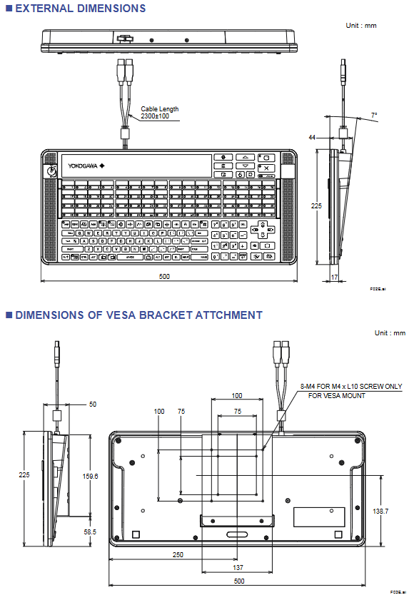
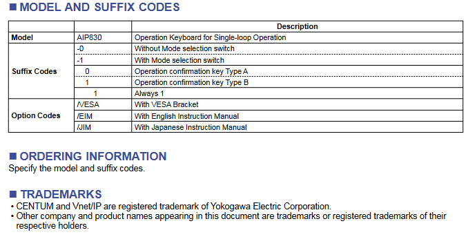
AIP830 is a single loop operation keyboard designed specifically for desktop HIS (Human Interface Station) by Yokogawa Electric Corporation. Its core application is process control and factory monitoring in industrial scenarios, and it can achieve key functions such as equipment operation, parameter setting, and alarm processing, providing a stable and efficient human-machine interaction solution for industrial automation systems. Each desktop HIS is only compatible with one AIP830 keyboard to ensure uniqueness and stability of operation.
(2) Product Core Features
Compared to conventional operation keyboards, AIP830 has dual audio functions: in addition to the traditional buzzer sounds, it is equipped with an independent USB speaker (sound function) that can provide clearer and more diverse audio feedback, meeting the differentiated needs of alarm prompts, operation confirmation, and other audio signals in industrial environments.
Detailed hardware specifications
(1) Basic types and interface parameters
Keyboard type: Flat panel keyboard, integrated USB speaker sound function, compact structure, suitable for industrial console installation scenarios.
PC interface configuration:
Interface type: 2 USB A-type interfaces (* 1 note: Both interfaces must always be directly connected to the PC and cannot be transferred through intermediate devices such as hubs to ensure signal transmission stability).
Compatible with USB standards: The keyboard function follows the USB 2.0 standard (full speed mode, bus powered), with stable data transfer rate, meeting the real-time operation command transmission requirements in industrial control; The sound function follows the USB 1.1 standard (full speed mode, bus powered) to ensure smooth output of audio signals.
(2) Power supply and power consumption parameters
Input voltage: 5V ± 5%, powered directly through the USB port of the PC, without the need for an additional power adapter, simplifying the installation process and reducing device deployment complexity.
Maximum current consumption: 1A, reasonable power consumption control, will not cause excessive load pressure on the PC power supply system, ensuring the stable operation of the entire equipment.
(3) Physical characteristics
Weight: The weight is 2.0kg without VESA bracket and 2.5kg with VESA bracket (* 2 note: AIP830 keyboard with VESA bracket must be installed in a position with a load-bearing capacity of not less than 10kg to prevent detachment after installation and ensure safe use).
Body color: black, with a color standard equivalent to Munsell No. N1.5. The appearance is simple and durable, suitable for the visual needs and anti pollution and wear-resistant requirements of industrial environments.
Installation category: Compliant with Class I installation category in IEC 61010-1 standard, it belongs to equipment that is not directly connected to the main power supply. The insulation protection design is more reliable and reduces safety risks in industrial electrical environments.
(4) Environmental adaptation parameters
Work environment:
Environmental temperature: 5 ℃~40 ℃ (normal operating temperature range), can adapt to the temperature conditions of most industrial plants and control rooms, without the need for additional constant temperature equipment.
Environmental humidity: 20%~80% RH (no condensation), to avoid internal short circuits and component corrosion caused by humidity changes, and ensure stable operation in humid or dry environments.
Storage and transportation environment:
Environmental temperature: -20 ℃~60 ℃, can withstand extreme temperature changes during long-distance transportation, as well as low or high temperature environments during long-term storage, reducing the risk of equipment damage when not in use.
(5) Size and cable specifications
External dimensions (unit: mm): The core dimensional parameters include length of 500mm, width of 225mm, height of 44mm, and detailed dimensions such as local protrusion height of 17mm. The compact size design facilitates installation and deployment within the limited space of the operating platform.
Cable length: 2300mm ± 100mm, longer cables can flexibly adapt to the installation distance between PC and keyboard, with a tolerance range of ± 100mm to ensure production consistency and ease of use.
VESA bracket installation dimensions (unit: mm):
Bracket hole specifications: Supports two standard VESA mounting hole distances of 75mm × 75mm and 100mm × 100mm, suitable for most industrial brackets on the market.
Screw requirements: Only M4 × L10 specification screws are supported, with a total of 8 mounting holes to ensure a secure connection between the bracket and keyboard, avoiding loosening caused by vibration.
Compliance standards
(1) Safety standards
Compatibility standards: CSA, CE Marking.
Compliance prerequisite: The AIP830 keyboard can only comply with the compliance requirements of this standard when the corresponding certification marks (CSA mark, CE mark) are marked on the connected PC device, ensuring the safety certification consistency of the entire system.
Compatibility standards: CE Marking, C-Tick Marking, KC Marking.
Compliance prerequisite: Consistent with safety standards, PC devices that need to be connected must be labeled with corresponding certification marks (CE mark, C-Tick mark, KC mark) to meet electromagnetic compatibility requirements, avoid electromagnetic interference generated during device operation affecting other industrial equipment, and resist interference from external electromagnetic signals on keyboard operations.
Exception: In the CE Marking standard, EN 61000-3-2 (harmonic current emission limits) and EN 61000-3-3 (voltage fluctuation and flicker limits) are not applicable to the AIP830 keyboard, as the design characteristics of the device do not require it to meet the requirements of these two sub standards.
(3) Standard reference source
For detailed technical requirements of all compliance standards, please refer to the “System Overview” document (document numbers: GS 33K01A10-50E, GS 33K01A20-50E), which provides system level compliance details and testing basis.
Keyboard layout and functional design
(1) Button composition and classification
The key layout of AIP830 keyboard is designed around the efficiency and convenience of industrial operations, covering the following core key types:
Basic input keys: alphanumeric keys (for text input and parameter setting needs), numeric keypad (for quick input of numerical parameters), cursor movement keys (for interface navigation and parameter adjustment).
Control function keys: control keys (core control operations such as device start stop and mode switching), operation confirmation keys (confirm input instructions, execute operations), buzzer reset key (clear alarm beep), alarm confirmation key (respond and confirm industrial system alarms), data input key (accurately input process parameters, equipment instructions), display key (switch display interface, retrieve equipment status information).
Function expansion button:
Dedicated window calling key: designed by functional grouping, it can quickly access different industrial control windows (such as parameter setting window, equipment monitoring window, alarm log window, etc.), reducing operation steps.
64 user-defined function keys: The core is used for process control and factory monitoring. Users can customize key functions according to actual process requirements (such as quickly switching production formulas, retrieving specific equipment parameters, executing preset operation processes, etc.), greatly improving operational efficiency.
Fn combination key: As a function extension trigger key, it works in conjunction with other keys to achieve additional functions.
Page keys, Clear screen key, Container window key: adapted to the operational requirements of industrial control interfaces, supporting multi page switching, interface cleaning, specific function window calling, etc.
Status indication and audio components: POWER indicator light (displaying keyboard power status), built-in electronic buzzer (alarm prompt), built-in USB speaker (sound function output).
Protective structure: Plastic cover, used to protect the core button area, prevent dust, oil, water droplets, etc. from entering the industrial environment, and extend the service life of the equipment.
(2) Optional configuration function (selected by suffix code)
Mode selection switch:
Postfix code -0: No mode selection switch, suitable for scenarios where there is no need to switch operating modes.
Suffix-1: Equipped with a mode selection switch, supporting quick switching between different operating modes (such as manual/automatic mode, edit/run mode, etc.), suitable for complex control requirements.
Operation confirmation keys symbol type:
The suffix code 0: Type A symbol meets the operational needs of specific regions or users.
Suffix code 1: Type B symbol, providing differentiated visual identification for operators to quickly recognize.
Fixed suffix code: All models include a fixed suffix code “1” to indicate product series consistency.
(3) Fn combination key extension function
Page up key+Fn key: Switch to the “volume control key”, which can adjust the volume of the built-in USB speaker to meet the audio needs of different environments (such as increasing the volume in noisy environments and decreasing the volume in quiet control rooms).
Cursor movement key+Fn key: Switch to the “scroll key” to control the scrolling operation of the industrial control interface, making it easy to view monitoring data, alarm logs, and other information on long pages.
Clear screen button+Fn button: activates the clear screen function, clears temporary data, pop ups, etc. on the current display interface, and restores the interface to a clean state; At the same time, it supports modifying hardware settings to enable the clear screen button to take effect directly without pressing the Fn key, adapting to different user operating habits.
(4) Specific version restrictions (R5.01 and R5.02 versions)
Function key limitation: Only supports the first 32 user-defined function keys (No.1 to No.32), the last 32 function keys are not available, suitable for simplified application scenarios with less demand for custom functions.
Button disabled: The Container window key is not available, and there is no need to use this feature in this version.
The “FIO (Fieldnetwork I/O) System General Specification Manual” (document number: GS 33K50F10-50E) released by Yokogawa Electric Corporation is the 8th edition updated in September 2014. Its core purpose is to guide the module selection, system deployment, installation, debugging, and compliance verification of the system in the CENTUM VP (Vnet/IP) integrated production control system. The FIO system, as a field I/O solution, focuses on the acquisition and control of industrial field signals. It is interconnected with field control units (FCUs) through multiple buses and is suitable for process control needs in industries such as petrochemicals, power, and pharmaceuticals.
System architecture and core components
(1) Overall architecture design
The FIO system adopts a layered architecture of “FCU+node unit+bus”, which realizes reliable interconnection between on-site signals and control units, supports dual redundancy configuration (power module, bus interface module, I/O module), and ensures high availability operation of industrial sites. The system can achieve chain or star topology expansion through the optical ESB bus relay unit (ANT10U), adapting to centralized and distributed deployment scenarios.
(2) Classification and specifications of core components
1. On site Control Unit (FCU)
FCU is the system control core, responsible for receiving on-site signals from FIO node units and executing control logic. The specific model and characteristics are as follows:
Model series type installation method adaptation bus core characteristics
AFV30 (S/D) standard/dual redundant 19 inch rack mounted ESB bus and optical ESB bus support node expansion package, connecting up to 13 node units
AFV40 (S/D) standard/dual redundant integrated ESB bus with cabinet, optical ESB bus. A single cabinet can install up to 11 node units and relay units
AFV10 (S/D) standard/dual redundant 19 inch rack mounted ESB bus, ER bus miniaturization design, suitable for small and medium-sized control scenarios
2. Node unit
Node units are interface carriers for on-site I/O signals, integrating power modules, bus interface modules, and I/O modules. They are divided into three categories according to the adapted bus:
Node unit type, model series, redundancy support, adaptation to bus core usage
ESB bus node unit ANB10 (S/D) single/dual redundant ESB bus close range (≤ 10m) on-site signal acquisition and transmission
Optical ESB bus node unit ANB11 (S/D) single/dual redundant optical ESB bus long-distance (up to 50km) anti-interference signal transmission
ER bus node unit ANR10 (S/D) single/dual redundant ER bus medium short distance (≤ 185m) economical signal transmission
3. Relay unit
Model Name Core Function Adaptation Scenarios
ANT10U optical ESB bus relay unit optical ESB bus chain/star expansion, amplifying optical signals for cross plant and long-distance node interconnection
4. Bus interface module
Used to achieve bus interconnection between FCU and node units, the key models and characteristics are as follows:
Model name adaptation bus core parameter installation requirements
EC401 ESB bus coupler module ESB bus single module can connect up to 9 node units AFV30 /AFV40 /AFV10 , which need to be installed in slots 7/8
EC402 2-port ESB bus coupler module, with 9 node units connected to each of the upper and lower ports of the ESB bus, is only compatible with AFV30/AFV40
The EB401 ER bus interface main module ER bus supports dual redundant communication. The single module is installed in odd numbered slots, and the slot on the right side needs to be left blank
ANT401/ANT411 Optical ESB Bus Relay Main Module Optical ESB Bus Transmission Distance 5km/5-50km Only compatible with AFV30 /AFV40
ANT502/ANT512 optical ESB bus relay module cooperates with the main module to achieve long-distance expansion, pre installed in the ANB11 node unit
Detailed Explanation of Bus System Specifications
The FIO system supports three types of buses: ESB, optical ESB, and ER, adapting to different distance and bandwidth requirements. The core specifications are as follows:
(1) ESB bus (AFV full series FCU adaptation)
Application scenario: Close range interconnection between FCU and local node units;
Transmission parameters: speed of 128 Mbps, bus topology, dual redundancy support;
Transmission medium: dedicated cable (YCB301), maximum transmission distance of 10m;
Connection capacity: AFV30 /AFV40 (LFS1700 database) up to 3 node units, with a maximum of 13 after expansion; AFV10 (LFS1500 database) has a maximum of 3 node units, and can be expanded to a maximum of 9.
(2) Optical ESB bus (AFV30 /AFV40 adaptation)
Application scenario: Long distance, anti-interference node interconnection;
Transmission distance: 10m without relay, up to 50km with ANT411 relay;
Connection capacity: Share node unit quota with ESB bus.
(3) ER bus (AFV10 adaptation)
Application scenario: Medium to short distance economic interconnection;
Transmission parameters: speed of 10 Mbps, bus topology, dual redundancy support;
Transmission medium: coaxial cable (YCB141/YCB311), which needs to be interconnected through YCB147/YCB149 bus adapters;
Transmission distance: YCB141 has a maximum length of 185m; when using mixed cables, it is necessary to meet the requirement of “YCB141 length+(185/500) × YCB311 length ≤ 185m”;
Connection capacity: up to 3 node units for AFV10 (LFS1500 database), up to 14 after expansion, and up to 8 node units for a single bus.
I/O module classification and core parameters
The FIO system I/O modules cover four categories: analog, digital, communication, and turbine machinery. They support isolation switch type and built-in isolation grid type, and are compatible with various field signals. The core classifications and parameters are as follows:
(1) Analog I/O module
It includes three types: non isolated, isolated, and channel isolated, supporting current, voltage, TC/mV, and RTD/PAT signals. Representative models are as follows:
Model Name Channel Number Signal Type Isolation Characteristics Power Consumption (5V DC/24V DC) Explosion proof Support
AAI141 analog input module 16 4-20 mA non isolated 310 mA/450 mA CSA/FM spark free type
AAV141 analog input module 16 1-5 V non isolated 350 mA/- CSA/FM spark free type
AAI143 analog input module 16 4-20 mA isolated 230 mA/540 mA Type i (intrinsic safety type)
AAI543 analog output module 16 4-20 mA isolated 230 mA/540 mA Type i (intrinsic safety type)
ASI133 built-in isolation barrier analog input module 4-20 mA isolation 150 mA/450 mA Type i (intrinsic safety type)
AST143 built-in isolation barrier TC/mV input module 16 TC, -100-150 mV isolation 150 mA/80 mA Type i (intrinsic safety type)
(2) Digital I/O module
Supports DC, AC, and relay outputs, partially compatible with NAMUR standards. Representative models are as follows:
Model Name Channel Number Signal Type Isolation Characteristics Power Consumption (5V DC) Explosion proof Support
ADV151 digital input module 32 24 V DC isolated 500 mA CSA/FM spark free type
ADV551 digital output module 32 24 V DC isolated 700 mA CSA/FM spark free type
ADV141 digital input module 16 100-120 V AC isolated 500 mA CSA/FM spark free type
ADR541 relay output module 16 24-110 V DC/100-240 V AC isolated 780 mA CSA/FM spark free type
ASD143 built-in isolation barrier digital input module 16 NAMUR compatible isolation 150 mA Type i (intrinsic safety type)
ASD533 built-in isolation barrier digital output module 8 U>12 V (I=40 mA) isolation 150 mA Type i (intrinsic safety type)
(3) Communication module
Support multiple industrial communication protocols to achieve interconnection with third-party devices:
Model Name Port Number Communication Protocol Rate Power Consumption (5V DC)
ALR111 serial communication module 2 RS-232C 1200 bps-115.2 kbps 500 mA
ALR121 serial communication module 2 RS-422/RS-485 1200 bps-115.2 kbps 500 mA
ALE111 Ethernet Communication Module 1 Ethernet 10 Mbps 500 mA
ALF111 Foundation Fieldbus Module 4 FF-H1 31.25 kbps 500 mA
ALP111/ALP121 PROFIBUS-DP module 1 PROFIBUS-DP -700 mA
(4) Turbomachinery specialized module
Suitable for turbomachinery control scenarios, the core models are as follows:
Model Name Channel Number Function Power Consumption (5V DC) Environment Support
AGS813 servo module 12 servo control 500 mA G3 support
AGP813 high-speed protection module 26 device security protection 900 mA G3 support
(5) Compatible module
Designed for upgrading the CENTUM V, CENTUM-XL, and µ XL systems, it can reuse existing cables. Representative models include AAP149 (pulse input), AAP849 (pulse input/analog output), and ADV859-ADV569 (ST compatible digital I/O).
Environmental and power specifications
(1) Environmental requirements
Environmental parameters, working status, transportation/storage status, special instructions
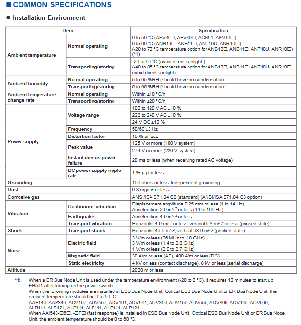
Temperature standard: 0-50 ℃ (AFV series)/0-60 ℃ (node unit); Wide temperature options: -20-70 ℃ Wide temperature options: -40-85 ℃ ER node unit -20-0 ℃ Start up requires 10 minutes of preheating
Humidity 5-95% RH (no condensation) 5-95% RH (no condensation)-
Temperature change rate ± 10 ℃/h ± 20 ℃/h-
Vibration 1-14Hz: displacement ≤ 0.25mm; 14-100Hz: acceleration ≤ 2.0 m/s ² Earthquake: horizontal ≤ 4.9 m/s ²; Vertical ≤ 9.8 m/s ² in packaging state
Dust ≤ 0.3 mg/m ³ —
Corrosive gas standard: ANSI/ISA S71.04 G2; Option: G3–
Electromagnetic environment electric field ≤ 3 V/m (26MHz-2GHz); Magnetic field ≤ 30 A/m (AC)/400 A/m (DC) —
Communication input: 100-120 V AC (± 10%) or 220-240 V AC (± 10%), frequency 50/60Hz (± 3Hz), distortion ≤ 10%, peak value ≥ 125 V (100V system)/274 V (220V system);
DC input: 24 V DC (± 10%), ripple rate ≤ 1% p-p;
Instantaneous power outage tolerance: ≤ 20ms (under rated AC voltage);
The General Overview Manual for Yokogawa Electric’s CENTUM VP Integrated Production Control System (Document Number: TI 33J01A10-01EN) is the 4th edition released in 2016, which provides a detailed introduction to the system’s core concepts, configuration architecture, functional characteristics, engineering environment, and full lifecycle support. As the 8th generation CENTUM series product, CENTUM VP is the core platform of Yokogawa VigilantPlant solution, designed for control and management of multi industry factories, with high reliability, openness, and flexible scalability.
Core philosophy and core advantages
(1) Core concept
Build a full value chain operation support system around the three dimensions of “See Clearly, Know in Advance, Act with Agility”:
See Clearly: Real time capture of factory wide data, precise push of key information, reducing information overload and blind spots;
Know in Advance: Integrate historical, real-time, and predictive data to support rapid and intelligent decision-making, and mitigate operational risks;
Act with Agility: Accelerate task collaboration, automate best practices, enhance production flexibility and bottleneck prediction capabilities.
(2) Core advantages (by role/scenario)
Description of core advantages of applicable objects/scenarios
Unified control/security/asset intelligence interface by operators to avoid information overload; Continuous Systematic Best Operating Practices
The integrated engineering environment of Engineer AD Suite supports flexible design, and the control application and I/O configuration can be independently adjusted
Production management is compatible with S95/B2MML standards, achieving MES/enterprise system integration; Built in network security authentication
Maintenance personnel upgrade and modify online without any single point of failure; 40 year downward compatibility, protecting long-term investments
Integrated solution for project implementation (DCS/SIS/PIMS, etc.) to reduce integration risks and accelerate project delivery
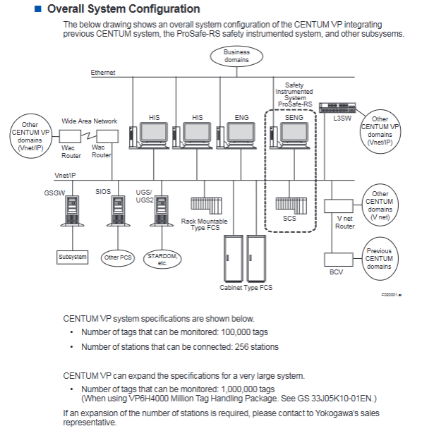
System configuration and core components
(1) Overall architecture
The system is centered around “HIS+FCS+control network” and supports full-scale deployment from small to super large (1 million tags). It can integrate security systems, third-party devices, and remote sites to form a unified control ecosystem.
(2) Key component description
core component
HIS (Human Interface Station): Based on Windows system, supports desktop/open/closed consoles, compatible with 16:10/4:3 displays, multiple HIS mutual backup without single point of failure;
FCS (Field Control Station): independently developed by Yokogawa, supporting cabinet/rack installation, equipped with dual redundant processors, power and I/O modules, supporting online maintenance and remote deployment (IEC Zone 2/Class I Div. 2);
Control network (Vnet/IP): 1Gbps redundant Ethernet, compliant with IEEE802.3 standard, supports 5ms full network time synchronization, ensuring deterministic communication.
Auxiliary components
ENG (Engineering Station): Install AD Suite engineering software, supporting modular/non modular engineering design;
Gateway station (GSGW/USGS/BIOS): GSGW is used for subsystem monitoring, UGS/UGS2 integrates STARDOM/PLC, SIOS connects to third-party PCS (OPC interface);
Communication relay devices: BCV (connecting old CENTUM system), AVR (interconnecting Vnet/IP and V net), WAC Router (connecting Vnet/IP domains across WAN).
integrated system
ProSafe-RS: T Ü V SIL3 certified safety instrumented system, supporting ESD/PSD/F&G/BMS functions, sharing operating environment with CENTUM VP to achieve integrated safety and control;
Digital fieldbus: supports mainstream protocols such as Foundation fieldbus, HART, PROFIBUS-DP, Modbus TCP/IP, ISA100.11a, etc;
Third party integration: Through OPC DA/A&E interface, data exchange with third-party PCS and ERP systems is achieved.
Detailed explanation of core functions
(1) Engineering Features (AD Suite)
AD Suite is an integrated engineering environment added to CENTUM VP R6, supporting full lifecycle engineering management. Its core functions are divided into standard and optional features
Function type, specific function, core value
The standard function non modular project first determines the hardware configuration, and then carries out engineering design on a hardware by hardware basis
History management automatically saves engineering change records, supports traceability and retrieval
AD Server centrally manages engineering data and projects, supports backup/recovery
Optional modular engineering reuse design modules (control logic/alarm attributes, etc.) to improve efficiency and consistency
Batch editing and modification of multiple module parameters, supporting consistency verification
Change control is managed through ModPack to manage the change process, recording test results and responsible parties
Dependency analysis analyzes the correlation between control logic/I/O/graphic labels and evaluates the impact of changes
Optimize parameter management by comparing design values with on-site actual values, supporting batch distribution and synchronization
(2) Control Function (FCS)
High reliability design: The processor, power supply, I/O module, and network are fully redundant, and the Pair&Spare architecture enables seamless fault switching;
Flexible control capability: supports adjustable control, advanced control, complex sequential control, and batch control, adapting to different scale requirements through functional block combinations;
Unit monitoring: defining multiple devices as a single unit for unified operation, simplifying batch and continuous process management;
Online maintenance: supports engineering data modification and module replacement without interrupting process control.
(3) Human Computer Interface Function (HIS)
Integrated operation: Integrate CENTUM VP control data, ProSafe RS security alerts, and PRM asset data to achieve seamless management;
Compliant design: Complies with EEMUA 191 alarm system design standards to reduce the risk of alarm storms;
Flexible display: Supports multi monitor deployment, with operation windows that can be moved across screens to adapt to different monitoring scenarios.
(4) Openness and Interoperability
Global HIST Network: Set up testing sites in Japan, the Netherlands, the United States, and Singapore to verify interoperability with non Yokogawa equipment;
High speed open network: Vnet/IP supports 1Gbps transmission and is compatible with TCP/IP, ensuring real-time data updates for large-scale projects;
Standard interface support: Implement information flow, advanced control, and alarm management with external systems through OPC servers.
Full lifecycle support
(1) Project Phase
Accurate cost estimation: FCS load can be calculated during the design phase, and label authorization is only divided into three levels: 8000 points (small), 100000 points (medium and large), and 1000000 points (multi factory interconnection), reducing change costs;
Virtual testing function: Control and operation functions can be tested without hardware, accelerating project progress and supporting the establishment of Operator Training System (OTS).
(2) Operation and Upgrade Phase
Convenient upgrade: PC based sites can be upgraded with just one click, and FCS can upgrade new features as needed without the need for mandatory updates;
Smooth migration: supports the migration of old CENTUM systems (such as CS3000, uXL) to third-party DCS, and can reuse assets such as on-site cables and I/O modules;
RIO system upgrade: The RIO system of CENTUM CS/CS3000/VP can be upgraded to the latest FCS (A2FV70 ) without changing the field equipment interface.
Key specifications of the system
Specific parameters of specification items
Maximum monitoring tag count of 1000000 points (requires VP6H4000 Million Tag Handling Package)
Maximum number of connected sites 256 (expandable, sales need to be contacted)
Control network speed 1Gbps (Vnet/IP)
Time synchronization accuracy 5ms (Vnet/IP network wide)
FCS availability 99.99999%
ProSafe RS safety system certification complies with IEC 61508 SIL3 standard
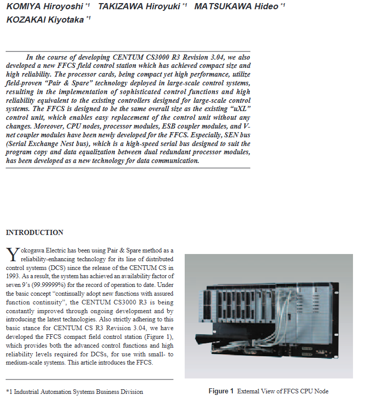
Yokogawa Electric released a technical report (No. 38) in 2004, focusing on the newly added FFCS compact field control station in the CENTUM CS3000 R3 V3.04 version. As a field control station (FCS) designed specifically for small and medium-sized systems, FFCS inherits the high reliability and advanced functions of large DCS, achieves compactness through a new hardware design, and is compatible with existing uXL systems, supporting low-cost upgrades, enriching the FCS product line of CENTUM CS3000 R3 (including standard, extended, renewable, and highly distributed types).
FFCS Core Features
Specific description of characteristic category
Compact and compatible volume is 1/5 of traditional control units; The external dimensions are consistent with the uXL control system control unit and can be directly replaced, maximizing the reuse of existing assets
High reliability adopts Pair&Spare dual redundancy technology, with no instantaneous switching control in case of failure; System availability reaches 7 9s (99.99999%)
Advanced features with complex control functions equivalent to large controllers, supporting system software reuse (common for small and medium-sized/large factories)
Scalable CPU nodes can install up to 8 I/O modules; Can connect up to 3 extension nodes (directly coupled nodes+remote nodes)
Hardware compatibility is compatible with the I/O module (IOM) and field network I/O module (FIO) of CENTUM CS3000 R3
Hardware configuration details
(1) Overall redundant architecture
FFCS supports full hardware dual redundancy configuration, with core redundant components including processor modules, power units (PW481/PW482/PW484), communication buses (SEN/ESB/ER/V-net), and I/O modules, ensuring that a single point of failure does not affect system operation.
(2) Core hardware components
CPU node
The smallest system core can run independently and can install up to 8 IOM modules;
Interface module: EC401 (ESB bus coupler) is required to connect directly coupled nodes, and EB401 (ER bus main interface module) is required to connect remote nodes.
Hardware Reuse: Integrated with CENTUM CS3000 mature CP345 processor card and SB301 interface card, software compatible;
Packaging form: Modular packaging (replacing traditional card design), built-in nickel hydrogen battery (environmentally friendly alternative to nickel cadmium battery), backup main memory;
Core function: Achieve fault free instantaneous switching and ensure control continuity.
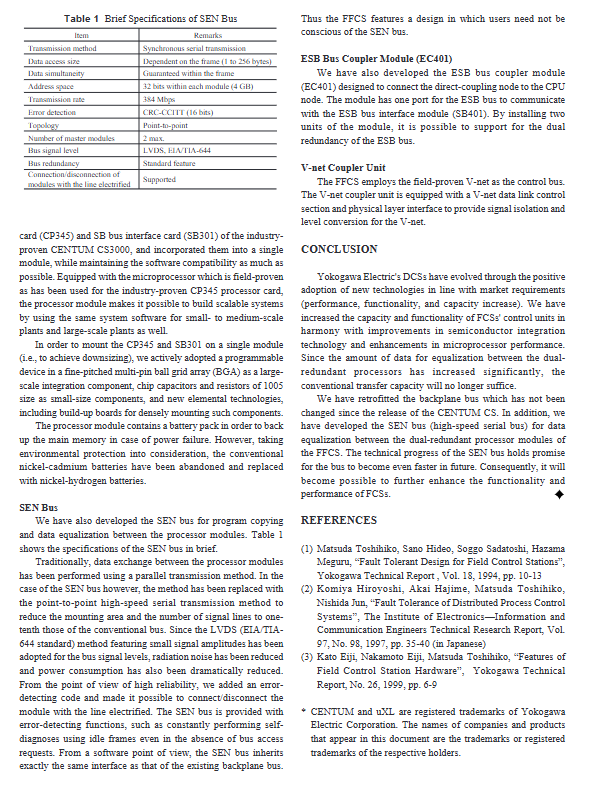
The SEN bus (Serial Exchange Nest bus) is specifically developed for program copying and data synchronization of dual redundant processor modules, with the following key parameters:
Specific specifications of parameter items
Transmission method: synchronous serial transmission
Transmission rate 384 Mbps
Data access size 1-256 bytes (depending on frame structure)
Live operation support module for live plugging and unplugging
Advantages: Compared to traditional parallel transmission, the signal line and installation area are reduced to 1/10, reducing radiation noise and power consumption.
Other key modules
EC401: ESB bus coupler module, 1 ESB bus port, dual module configuration supports ESB bus redundancy;
V-net coupling unit: integrates V-net data link control and physical layer interface to achieve signal isolation and level conversion;
EB401/EB501: ER bus master/slave interface module, used to connect remote nodes;
SB401: The ESB bus is an interface module used to expand communication between nodes and CPU nodes.
System configuration and connection
Minimum system: Only CPU nodes (including 8 IOM modules) meet basic control requirements;
Expansion system: CPU nodes+up to 3 expansion nodes (directly coupled nodes/remote nodes) to expand I/O capacity;
Adaptation scenario: Distributed control requirements for small and medium-sized factories, especially suitable for space constrained and high reliability scenarios;
Upgrade value: uXL system users can directly replace control units, minimize equipment investment, and reuse existing assets;
Technical value: The SEN bus lays the foundation for subsequent FCS functional upgrades (such as greater data synchronization), and the dual redundancy design ensures production continuity.
Key issues
Question 1: How can the FFCS compact on-site control station achieve compact design while ensuring reliability and control functions comparable to large DCS?
Answer: ① Reliability guarantee: Adopting Yokogawa’s mature Pair&Spare dual redundancy technology, the processor module dual MPU synchronous calculation+cross validation, no instantaneous switching control in case of failure, system availability reaches 7 9s (99.99999%), consistent with large DCS; ② Functional reuse: Integrate the validated CP345 processor card and SB301 interface card core assets of CENTUM CS3000 on hardware, and universal system software at the software level to ensure consistent complex control functions; ③ Compact implementation: Adopting high-density installation technologies such as BGA packaging programmable devices, 1005 size components, and multilayer boards, multiple traditional card components are integrated into a single modular package, compressing the volume to 1/5 of traditional control units.
Question 2: What are the core technical advantages of FFCS’s SEN bus compared to traditional parallel transmission buses? What practical value do these advantages bring to the operation of the system?
Answer: The core advantages and practical value are as follows: ① Transmission performance: With a speed of 384 Mbps, it meets the large data synchronization requirements of dual redundant processors and solves the problem of insufficient transmission capacity of traditional buses; ② Hardware optimization: point-to-point serial transmission, reducing signal lines and installation area to 1/10, reducing hardware costs and space occupation; ③ Stability improvement: Adopting LVDS level standard, with low radiation noise and low power consumption, combined with CRC-CCITT error detection and idle frame self diagnosis function, to improve transmission reliability; ④ Convenient operation and maintenance: supports module live plugging and unplugging, maintenance can be carried out without stopping the machine, reducing the risk of production interruption; ⑤ Compatibility: Inheriting the existing backplane bus software interface, users can use it without additional adaptation.
Question 3: What are the core advantages of upgrading to FFCS for existing uXL control system users? What hardware compatibility issues should be noted during the upgrade process?
Answer: Core upgrade advantages: ① Seamless replacement: FFCS has the same external dimensions as the uXL control unit and can be directly replaced without changing the installation structure, maximizing the reuse of existing assets; ② Performance improvement: Achieve high reliability (dual redundancy) and advanced control functions equivalent to large DCS, meeting higher production requirements; ③ Flexible Expansion: Supports up to 3 expansion nodes and 8 I/O modules, and can be flexibly expanded according to production scale. Compatibility issues to be noted: ① Power supply unit: Use the PW481/PW482/PW484 models specified in the document to ensure power supply matching; ② I/O module: Only compatible with the IOM (I/O module) and FIO (Field Network I/O module) of the CENTUM CS3000 R3 series. It is necessary to confirm whether the existing module belongs to this series; ③ Expansion interface: When connecting expansion nodes, dedicated interface modules such as EC401 and EB401 must be used in conjunction, and other types of interface cards cannot be mixed.
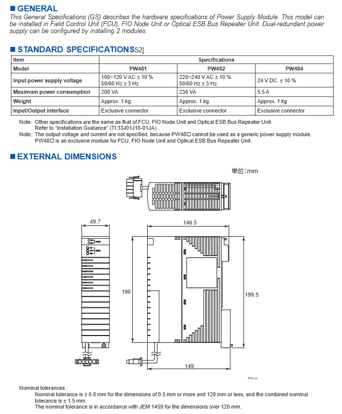
Positioning: This document is the General Specification Manual (GS 33J60E70-01EN) for Yokogawa Electric’s PW481, PW482, and PW484 series power modules. It was released in January 2021 and is the first edition. Its core purpose is to provide technical guidance such as module hardware parameters, installation specifications, and ordering information.
Product positioning: This series of modules is an exclusive power module and cannot be used as a universal power supply. It is only compatible with the control units and relay units specified by Yokogawa.
Details of Core Technical Parameters
The core parameter differences of the three modules are concentrated in the input power specifications, while the other key physical and interface parameters are consistent, as shown in the table below:
Parameter item PW481 PW482 PW484
Input power supply voltage 100~120 V AC ± 10% 220~240 V AC ± 10% 24 V DC ± 10%
Input power frequency 50/60 Hz ± 3 Hz 50/60 Hz ± 3 Hz None (DC input)
Maximum power consumption 200 VA 230 VA 5.5 A
Weight approximately 1 kg, approximately 1 kg, approximately 1 kg
Output parameter description without clear labeling (exclusive adaptation, dependent on target device) without clear labeling (exclusive adaptation, dependent on target device) without clear labeling (exclusive adaptation, dependent on target device)
Core features: AC input, non universal power AC input, non universal power DC input, non universal power supply
Installation specifications and compatible equipment
Adaptation installation unit
FCU (Field Control Unit): AFV30D, AFV30S, A2FV50D, A2FV50S, A2FV70D, A2FV70S
FIO Node Unit: ANB10D, ANB10S, ANB11D, ANB11S
Optical ESB Bus Repeater Unit: ANT10U
Base Plate: A2BE1D, A2BE2D
Installation restrictions (key requirements)
Slot requirements: must be installed in slots P1-P2;
Single module configuration: can only be installed in slot P1;
Dual redundancy configuration: Two identical modules (including suffix codes) need to be installed.
Model coding rules (suffix code description)
The suffix code rules for the three modules are completely consistent, used to distinguish between explosion-proof levels and special function options, as shown in the following table:
The suffix code function description applies to all models
-5 standard type, without explosion-proof protection
-E standard type, with explosion-proof protection
0 basic type (without additional functional options) is
1 with ISA Standard G3 option, suitable for temperature range -20 ℃~70 ℃
Ordering and Applicable Standards
Ordering requirements: When ordering, it is necessary to clearly specify the “module model+suffix code”, for example, “PW481-E-1” represents a power module with 100-120V AC input, explosion-proof protection, support for ISA G3 standard and wide temperature range.
Explosion proof selection: If it needs to be used in explosion-proof scenarios, it is necessary to refer to the related document “TI 33Q01J30-01E” to confirm the compliance of the selection.
Applicable standards: The module as a whole follows the relevant standards in the Integrated Production Control System CENTUM VP System Overview (document number: GS 33J01A10-01EN).
Module classification and core technical parameters
The document categorizes NFA series modules into two main types based on “isolation characteristics” and “functional types”, each containing multiple sub models. The core parameters are as follows:
(1) Non isolated module
Non isolated modules have no electrical isolation design between input/output and the system, suitable for scenarios with low isolation requirements, mainly including current/voltage input modules and current/voltage I/O modules.
1. Current/voltage input module (non isolated)
Model NFAI141 NFAV141
Channel configuration: 16 channels, non isolated 16 channels, non isolated (differential input)
Input signal 4~20 mA DC 1~5 V DC (allowing common mode voltage ± 1 V)
Allow input value of 27 mA ± 7.5 V
No overcurrent protection available
Input resistance power on: 250 Ω (internal protection circuit may generate a maximum voltage drop of 3 V); Power off: ≥ 500 k Ω Power on: ≥ 1 M Ω Power off: ≥ 340 k Ω
Core accuracy ± 0.1% full-scale ± 0.1% full-scale
Response performance data refresh cycle: 10 ms; Input step response time: 100 ms Data refresh cycle: 10 ms; Input step response time: 100 ms
The transmitter power supply is 22.8-26.4 V DC (with an output current limit of 27 mA), and it needs to be powered by a 24 V DC analog field power supply through the base module
Channel settings support 2-wire/4-wire transmitters, configured separately by pin
Temperature drift maximum ± 0.01%/° C maximum ± 0.01%/° C
Power consumption 5 V DC: 310 mA; 24 V DC:450 mA 5 V DC:350 mA; 24 V DC: None
Weight 0.2 kg 0.2 kg
External connection pressure clamping terminal, MIL connector cable pressure clamping terminal, MIL connector cable
Special features support HART communication; Do not connect the Zener barrier. For intrinsic safety applications, an isolation barrier without HART communication function is required
2. Current/voltage I/O module (non isolated)
Supports 8 inputs and 8 outputs, can adapt to 8 control circuits, core models are NFAI841 and NFAB841, key parameters are as follows:
Model NFAI841 NFAB841
Channel configuration: 8-in/8-out, non isolated 8-in/8-out, non isolated (differential input)
I/O signal input: 4~20 mA; output: 4~20 mA; input: 1~5 V (common mode voltage ± 1 V); Output: 4~20 mA
Allow input value of 25 mA ± 7.5 V
No overcurrent protection available
Input resistance powered on: 250 Ω; Power off: ≥ 500 k Ω Power on: ≥ 1 M Ω Power off: ≥ 340 k Ω
Wire breakage detection output wire breakage detection threshold ≤ 0.65 mA output wire breakage detection threshold ≤ 0.65 mA
Core precision input: ± 0.1% full scale; Output: ± 0.3% full-scale input: ± 0.1% full-scale; Output: ± 0.3% full scale
Response performance data refresh cycle: 10 ms; input step response time: 100 ms; output step response time: 40 ms consistent with NFAI841
Output Fallback configured by channel (HOLD: Maintain fault output; SETV: output specified value), detection time of 4 seconds is consistent with NFAI841
The transmitter power supply is 22.8-26.4 V DC (with a current limit of 27 mA), and an external 24 V DC supply is required
Channel settings: 2-wire/4-wire transmitters are configured separately by pin. None available
Temperature drift maximum ± 0.01%/° C maximum ± 0.01%/° C
Power consumption 5 V DC: 310 mA; 24 V DC:500 mA 5 V DC:310 mA; 24 V DC:250 mA
Weight 0.3 kg 0.3 kg
External connection pressure clamping terminal, MIL connector cable pressure clamping terminal, MIL connector cable
Special features support HART communication; Prohibit connection to Zener barrier without HART communication function
(2) Isolation type module
Isolation modules have electrical isolation between input/output and system or channel, with stronger anti-interference ability, suitable for complex industrial environments, covering various types such as current/voltage input/output, TC/RTD input, pulse/frequency input, etc.
1. Current input/output module (isolated)
Model NFAI143 (current input) NFAI543 (current output)
Voltage resistance performance between input and system: 1500 V AC/1 minute (500 V AC/1 minute when using KMS40 cable) Output and system: 1500 V AC/1 minute (500 V AC/1 minute when using KMS40 cable)
No overcurrent protection available
Input/output resistance input power on: 250 Ω; Power off: ≥ 500 k Ω without clear input resistance parameters
Core accuracy ± 0.1% full-scale ± 0.3% full-scale
Response performance data refresh cycle: 10 ms; Input step response time: 100 ms Data refresh cycle: 10 ms; Output step response time: 100 ms
Output Fallback without channel configuration (HOLD/SETV), detection time 4 seconds
The transmitter power supply is 24.0~25.5 V DC (with a current limit of 25 mA), and an external supply of 24 V DC is required
Channel settings: 2-wire/4-wire transmitters are configured separately by pin. None available
Temperature drift maximum ± 0.01%/° C maximum ± 0.01%/° C
Power consumption 5 V DC: 230 mA; 24 V DC:540 mA 5 V DC:230 mA; 24 V DC:540 mA
Weight 0.3 kg 0.4 kg
External connection pressure clamping terminal, MIL connector cable pressure clamping terminal, MIL connector cable
Special features support HART communication; Prohibit the connection of Zener barriers to support HART communication; Do not connect the Zener barrier
2. Voltage input/output module (isolated)
Model NFAV144 (voltage input) NFAV544 (voltage output)
I/O signal input: 1~5 V/-10~+10 V (uniformly set for all channels, -10~+10 V can be adjusted by the resource configurator) Output: -10~+10 V DC
Allowable Input/Load Allowable Input Voltage: -30~+30 V Allowable Load Resistance: ≥ 5 k Ω
Voltage resistance performance between input and system: 1500 V AC/1 minute (KMS40 cable: 500 V AC/1 minute) Output and system: 1500 V AC/1 minute (KMS40 cable: 500 V AC/1 minute)
Input/output resistance power on: 1 M Ω; power off: 200 k Ω No clear output resistance parameters
Core accuracy ± 0.1% full-scale ± 0.3% full-scale
Response performance data refresh cycle: 10 ms; Input step response time: 100 ms Data refresh cycle: 10 ms; Output step response time: 40 ms
Output Fallback without channel configuration (HOLD/SETV), detection time 4 seconds
Temperature drift maximum ± 0.01%/° C maximum ± 0.01%/° C
Power consumption 5 V DC: 500 mA; 24 V DC: No 5 V DC: 860 mA; 24 V DC: None
Weight 0.2 kg 0.2 kg
External connection pressure clamping terminal, MIL connector cable pressure clamping terminal, MIL connector cable
Special functions without HART communication; Wide range adaptation without HART communication; High load resistance requirement
3. TC/RTD input module (isolated)
Specially designed to receive thermocouple (TC), thermistor (RTD), or millivolt (mV) signals, suitable for temperature measurement scenarios, the core models are NFAT141 (TC/mV input) and NFAR181 (RTD input).
Input signal TC: JIS C1602, IEC60584 standard Type J/K/E/B/R/S/T/N (Type B without temperature compensation, measured at ≥ 44 ℃); MV: -100~150 mV, -20~80 mV RTD: JIS C1604, IEC60751 standard Pt100 (three wire system), JIS C1604 standard JPt100 (three wire system)
Signal switching TC/mV can be set separately by channel (CH1~CH16) None
Allow input voltage ± 5 V ± 5 V
Voltage resistance performance between input and system: 1500 V AC/1 minute (MIL cable must meet corresponding voltage resistance requirements) Input and system: 1500 V AC/1 minute
Input resistance power on/off: ≥ 2 M Ω No clear parameters
Core precision TC input: ± 0.03% of full scale (-20~80 mV); MV input: ± 0.032% full range (-100~150 mV) ± 0.03% full range (0~400 Ω)
Allow total resistance signal source+wiring total resistance ≤ 1000 Ω, single wiring resistance ≤ 40 Ω, and each wire resistance is equal
Reference compensation accuracy ± 1 ℃ (affected by installation environment: ± 2 ℃ at -20~15 ℃/45~70 ℃; ± 1 ℃ at 15~45 ℃), coefficient K is required for temperatures below 0 ℃ (RTD does not require reference compensation)
Measuring current without 1 mA
Temperature drift TC input: maximum ± 30 ppm/° C; mV input: maximum ± 32 ppm/° C, maximum ± 30 ppm/° C
Data refresh cycle 1 second 1 second
The burn detection is uniformly set for all channels (enabled/disabled), with a detection time of 60 seconds
Power consumption 5 V DC: 450 mA; 24 V DC: No 5 V DC: 450 mA; 24 V DC: None
Weight 0.2 kg 0.2 kg
External connection pressure clamping terminal; Only mV input supports MIL connector cable pressure clamping terminal
Install restrictions to avoid radiation heat and direct airflow; Not adjacent to the CPU/power module; Can only be installed adjacent to designated modules (NFAT141/NFAR181/NFAV141/NFAV144) without special installation restrictions
4. Channel isolated current input/I/O module
The module not only has isolation between input/output and system, but also supports channel isolation, with stronger anti-interference ability. The core models are NFAI135 (current input) and NFAI835 (current I/O).
Model NFAI135 (current input) NFAI835 (current I/O)
I/O signal input: 4~20 mA input: 4~20 mA; output: 4~20 mA
Allow input current of 25 mA
Overcurrent protection is equipped with
Voltage resistance performance between input and system, channel: 500 V AC/1 minute (MIL cable must meet voltage resistance requirements) Input/output and system, channel: 500 V AC/1 minute
Input resistance power on: 250 Ω (internal protection circuit may generate a maximum voltage drop of 0.8 V); Power off: ≥ 500 k Ω consistent with NFAI135
Allow no output of load resistance: 0~750 Ω
Wire breakage detection without output. Wire breakage detection threshold ≤ 0.65 mA
Response performance data refresh cycle: 10 ms; input step response time: 100 ms Data refresh cycle: 10 ms; input/output step response time: 100 ms
Output Fallback without channel configuration (HOLD/SETV), detection time 4 seconds
The transmitter power supply is 20.2~29.3 V DC, which requires an external supply of 24 V DC
Temperature drift maximum ± 0.01%/° C maximum ± 0.01%/° C
Power consumption 5 V DC: 360 mA; 24 V DC:450 mA 5 V DC:360 mA; 24 V DC:450 mA
Weight 0.3 kg 0.3 kg
External connection pressure clamping terminal, MIL connector cable pressure clamping terminal, MIL connector cable
Special features support HART communication; Prohibit the connection of Zener barriers to support HART communication; Do not connect the Zener barrier
5. Pulse input module (isolated channel)
The model is NFAP135, which supports contact switching, voltage pulse, and current pulse inputs. The channels and systems are isolated, making it suitable for pulse counting scenarios.
Input signal: 2-wire system (contact ON/OFF, voltage pulse, current pulse, can provide transmitter power), 3-wire system (power supply type voltage pulse);
Input frequency: 0~10 kHz (with changes in wiring capacitance during dry contact pulse input: 0~800 Hz at 1000 pF, 0~350 Hz at 10000 pF, 0~180 Hz at 30000 pF);
Minimum pulse width: 40 μ s (with capacitance variation: 625 μ s at 1000 pF, 1.43 ms at 10000 pF, 2.78 ms at 30000 pF when dry contact pulse input);
Signal level: Contact input (open circuit ≥ 100 k Ω, closed circuit ≤ 200 Ω); Voltage pulse (VH: 3-24 V, VL: -1~8 V, swing ≥ 3 V); Signal source resistance ≤ 1 k Ω;
Resistance configuration: shunt resistor (OFF/200/500/1000 Ω, open circuit when powered off); Pull up resistor (68 k Ω, 12/24 V DC);
Core function: Supports anti shake filtering (dry contact signals below 10 Hz); The transmitter power supply can be selected as 12/24 V DC (with a current limit of 40 mA for 12 V and 30 mA for 24 V);
Response performance: Data refresh cycle of 2 ms;
Power consumption: 5 V DC: 300 mA; 24 V DC:400 mA;
Weight: 0.3 kg;
External connections: pressure clamping terminals, MIL connector cables;
Installation restriction: When selecting a 500 Ω shunt resistor, no other modules can be installed next to the module, and a maximum of 4 input channels can be used;
Input modes: 5 modes (dry contact pulse/relay contact/voltage pulse/2-wire current pulse/3-wire voltage pulse), requiring corresponding configuration of power supply and shunt resistor.
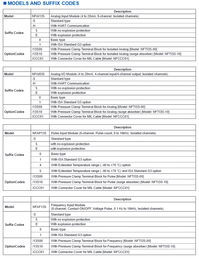
6. Frequency input module (isolated channel)
The model is NFAF135, used for measuring pulses and converting them into speed or frequency, with isolation between channels and systems.
Input signal: Contact ON/OFF, voltage pulse (rectangular wave);
Input frequency: 0.1 Hz~10 kHz (varies with capacitance when dry contact pulse input: 0.1~800 Hz at 1000 pF, 0.1~350 Hz at 10000 pF, and 0.1~180 Hz at 30000 pF);
Frequency accuracy: 0.1% reading;
Signal level: consistent with NFAP135;
Resistance configuration: shunt resistor (OFF/1000 Ω, open circuit when powered off); Pull up resistor (68 k Ω, 12/24 V DC);
Core function: The on-site power supply can be selected as 12/24 V DC (with a current limit of 40 mA for 12 V and 30 mA for 24 V), and external 24 V DC is required;
Response performance: data refresh cycle of 10 ms;
Power consumption: 5 V DC: 300 mA; 24 V DC:400 mA;
Weight: 0.3 kg;
External connections: pressure clamping terminals, MIL connector cables;
Input mode: 3 modes (dry contact pulse/relay contact/voltage pulse), corresponding to the configuration of power supply and shunt resistor.
General technical characteristics and physical parameters
(1) General performance parameters
Accuracy level: Input modules are generally ± 0.1% full scale, output modules are mostly ± 0.3% full scale, and TC/RTD modules have higher accuracy (± 0.03%~± 0.032% full scale);
Temperature stability: Most modules have a temperature drift of ≤± 0.01%/° C or ± 30-32 ppm/° C, suitable for industrial environment temperature changes;
Power requirements: All modules require a 5 V DC system power supply, and some modules (such as current input/output modules) require an additional 24 V DC analog field power supply, which must be applied through the base module;
Voltage resistance and protection: The voltage resistance between the input/output of isolation modules and the system is mostly 1500 V AC/1 minute, while the voltage resistance between channels of channel isolation modules is 500 V AC/1 minute. The voltage resistance of MIL connector cables depends on the cable specifications (such as KMS40 cables with 500 V AC/1 minute);
Intrinsic safety requirements: All modules are prohibited from connecting to Zener barriers, and isolation barriers must be used in intrinsic safety application scenarios.
(2) Physical and Connection Parameters
Dimensions: All modules have a uniform size of 107.5 mm x 32.8 mm x 130 mm (length x width x height, unit: mm);
Weight: Most modules weigh 0.2~0.4 kg, with non isolated modules generally lighter (0.2 kg) and isolated output modules slightly heavier (such as NFAI543 which weighs 0.4 kg);
External connection: Unified use of pressure clamping terminals and MIL connector cables, some modules (such as NFAR181) only support pressure clamping terminals;
LED status indicator: All modules are equipped with 3 green LED indicator lights:
Status: Illuminates when hardware is normal;
ACT: Illuminates when executing input/output actions;
DX: Not used (permanently extinguished).
Model coding rules
The module model consists of “basic model+suffix code+option code”, and the coding rules are as follows for easy selection and order confirmation:
(1) Basic model
The core functions and channel configurations of the representative module, such as NFAI141 (16 channel non isolated current input), NFAP135 (8-channel isolated pulse input), etc., have been explained in detail earlier.
(2) Suffix code
Used to distinguish the communication function, explosion-proof level, and special options of modules:
Example of applicable modules for suffix code function description
-S standard type (no special function) all models
-H supports HART communication NFAI141, NFAI841, etc
5. All models without explosion-proof protection
E with explosion-proof protection for all models
0 Basic type (no additional options) All models
1 with ISA Standard G3 option for all models
4 Wide Temperature Range Options (-40~+70 ℃) NFAP135, NFAR181
5 Wide Temperature Range+ISA Standard G3 Combination Options NFAP135, NFAR181
(3) Option code
Accessories such as terminal blocks and cable sheaths for specified modules:
/T4S10 Thermocouple/mV Special Pressure Clamp Terminal Block with Surge Absorber (Model: NFTT4S-10) NFAT141
/R8S00 RTD special pressure clamping terminal block (model: NFTR8S-00) NFAR181
/R8S10 RTD specific pressure clamping terminal block with surge absorber (model: NFTR8S-10) NFAR181
/A4S00 analog signal dedicated pressure clamping terminal block (model: NFTA4S-00) voltage input/output module
/A4S10 Analog Signal Special Pressure Clamp Terminal Block with Surge Absorber (Model: NFTA4S-10) Voltage Input/Output Module
/CCC01 MIL cable connector sheath (model: NFCCC01) All modules that support MIL cables
Installation restrictions and precautions
(1) Special module installation restrictions
NFAT141 (TC input module):
Avoid radiation heat effects: Do not install heating units below and do not expose them to direct airflow;
Module layout: Cannot be adjacent to CPU modules (NFCP501/NFCP502) or power modules (NFPW44x);
Adjacent module restriction: It can only be installed adjacent to NFAT141, NFAR181, NFAV141, and NFAV144, and at least one empty slot must be reserved for other modules.
NFAP135 (Pulse Input Module):
Partial current resistor limitation: When selecting a 500 Ω partial current resistor, no other modules can be installed on both sides of the module, and a maximum of 4 input channels can be used.
(2) General installation requirements
Power capacity matching: When installing modules, it is necessary to ensure that the total power consumption does not exceed the rated output of the power module, with a focus on:
5 V DC system power supply: current consumption of NFAV544, NFDV551, NFDV561, NFDR541;
24 V DC simulated on-site power supply: NFAI841, NFAI143, NFAI543 current consumption.
Explosion proof selection: Modules with the suffix “E” must be selected for explosion-proof scenarios, and the compliance of the selection must be confirmed by referring to the STARDOM FCN/FCJ Installation Guide.
Wiring and Connection:
Follow the requirements of the “On site Connection Specification” (GS 34P02Q30-01E) to ensure that the wiring is firm and the shielding is good;
The voltage resistance of MIL connector cables must meet the requirements of the module to avoid insufficient voltage resistance caused by improper cable selection.
Module Type Single Redundancy (AFV40S) Double Redundancy (AFV40D) Key Description
1 power module (PW481/PW482/PW484), 2 optional dual power supplies (redundant configuration) supporting 100-120V AC/220-240V AC/24V DC
1 processor module (CP461/CP471) 2 (redundant of the same model) CP471 needs to be equipped with R6.05 or above control functions
1 ESB bus coupling module (EC401/EC402), optional dual redundancy 2 (EC401/EC402, mandatory dual redundancy) EC401 can connect up to 9 nodes, EC402 can connect up to 11 nodes
Up to 6 I/O modules (non-standard configuration) must comply with the FIO system installation restrictions
2. Built in components of the cabinet
Basic components: 1 FCU, 1 power distribution board with HKU, 2 vertical power bus units (1 front and 1 rear)
Cooling components: 4 door fans (2 for each front and rear door), node fans (ANFAN, configured according to the number of units)
Core characteristics of interface type redundancy configuration
Vnet/IP interface dual redundancy (AFV40S selectable power supply, AFV40D forced dual power supply) system control network, redundant switching ensures stable communication
ESB bus interface AFV40S: single/dual redundancy; AFV40D: Mandatory dual redundant connection node unit, EC401 supports bus topology, EC402 supports upper and lower connection nodes
The HK bus interface is connected to the external cabinet HKU via a single channel, with AKBHKU cable and a total length of ≤ 100m
Software requirements: A separate software license is required. We recommend VP6F1700 control function software and VP6F3100 Project I/O license
SEM functional requirements: The use of event sequence manager requires specific hardware conditions, refer to GS 33J30D10-01EN
Standard accessories: 2 door fan filters (Part No.T9070CB)
Related products: Cabinet Connection Kit (Model AKT211), Cabinet Side Panel (ACB2P, requires paired configuration)
Key issues
Question 1: What is the core difference between AFV40S and AFV40D? How to select based on project redundancy requirements?
answer
Core Differences:
Redundancy configuration: AFV40S is single redundancy (optional dual redundancy for processor/power/ESB bus), AFV40D is full dual redundancy (mandatory dual redundancy for processor/power/Vnet/IP/ESB bus);
Suffix restrictions: AFV40D only supports dual redundancy related suffixes (such as ESB bus with only 2/4 options), while AFV40S supports single/dual redundancy suffixes;
Node Unit: AFV40S supports single/dual power node units, while AFV40D only supports dual redundant ESB+dual power node units (ANB10D-4 5).
Selection principle:
High reliability requirements (such as critical process control): Choose AFV40D, fully redundant configuration to avoid single point of failure;
Cost sensitive and non critical scenarios: Choose AFV40S and configure single/dual redundant ESB buses and power supplies as needed;
Number of nodes ≤ 9: AFV40S with EC401; Number of nodes 10-11: AFV40S with EC402, AFV40D with EC402.
Question 2: What are the key rules for unit installation and fan configuration in the AFV40 cabinet? How to avoid installation violations?
answer
Unit installation rules:
Quantity limit: A maximum of 11 units (ANB10 +ANT10U) can be installed in the cabinet, with ≤ 5 units in the front and ≤ 6 units in the rear;
Installation sequence: ANB10 node unit must be installed first, followed by ANT10U optical relay unit;
Cable connection: The ESB bus cable (YCB301) inside the cabinet has been pre installed, and manual connection is required between ANB10 and ANT10U.
Fan configuration rules:
The number of node fans (ANFAN) is configured according to the total number of units (0-4 → 1, 5-9 → 2, 10 → 3, 11 → 4);
Door fans are standard configuration (4 units), no additional selection is required.
Avoid violations:
Install strictly in the order of “ANB10 priority”, without reversing unit types;
Accurately select fan option codes based on the total number of units, without omission or excessive configuration;
The optical ESB node needs to be connected through the ANT401/ANT411 relay module, not directly connected to the FCU.
Question 3: What are the communication interface and power configuration options for AFV40? How to adapt to different on-site power supply conditions?
answer
Communication interface selection:
Vnet/IP interface: dual redundant configuration (AFV40S can provide a single power supply, AFV40D requires dual power supply), used for system control network;
ESB bus interface: AFV40S can be selected as a single menu (EC401/EC402 × 1) or dual redundancy (EC401/EC402 × 2), AFV40D is mandatory dual redundancy, used to connect node units;
HK bus interface: single channel, used to connect external cabinet HKU, total length ≤ 100m.
Power configuration selection:
Power supply type: Supports 100-120V AC (50/60Hz), 220-240V AC (50/60Hz), 24V DC, specified by suffix code;
Power redundancy: AFV40S can provide single/dual power supply, while AFV40D requires dual power supply.
On site adaptation plan:
Conventional industrial power supply (220-240V AC): choose suffix “2”, AFV40S can be a single power supply (suffix “3”) or a dual power supply (suffix “4”);
Low voltage scenario (24V DC): Select suffix “4” and confirm that the on-site DC power supply capacity is ≥ 71A;
Cross border project: Select option code “/CE” to obtain CE/RCM/ECC/KC multi certification adaptation;
Explosion proof scenario: Select option code “/ATDOC” to obtain the ATEX Directive Adaptation Manual.
ZWOPID (Wireless PID Compensation) is compatible with wireless field devices and provides PID control for stable process response in wireless communication scenarios when data packets are lost
YS instrument block compatible with YS series controllers/manual stations/total meters YS series instrument integrated control
Enhanced switch instrument block supports 1-2 input/output channels, including single trigger output type complex interlocking logic control
I/O function and communication support
1. Classification of I/O functions
I/O Type Core Function Signal Identification/Support Range
Process I/O on-site device signal interaction simulation I/O ≤ 1760 points, contact I/O ≤ 4096 points
Note: The suffix “11” represents the English version, and the extended license only supports upward upgrades (not downgrades)
Key issues
Question 1: What are the core differences between the three capacity configurations (C01/C02/C03) of VP6F1900/1905? How to select based on project requirements?
answer
Core difference: The number of labels (all 18000) and I/O points (all analog 1760 points/contact 4096 points) for the three types of configurations are completely the same, only the number of functional blocks and the number of control drawing options are different:
Standard type (C01): 5500 functional blocks, 200 control graphics (non expandable);
Expansion type (C02): 7000 functional blocks, 200 control graphics (optional 300/400/500);
Large type (C03): 9000 functional blocks, 200 control graphics (optional 300/400/500).
Selection principle:
Small projects (≤ 5500 functional blocks, ≤ 200 control graphics): Choose C01 standard type;
Medium sized project (function blocks 5501-7000, control drawing needs to be expanded): choose C02 expansion type;
Large scale projects (7001-9000 functional blocks, complex control logic): Choose C03 large type;
Possible future expansion: prioritize CO2/C03, or upgrade from C01 through an extended license.
Question 2: Features of VP6F1900 (N-IO compatibility Late Binding、 What engineering pain points does wireless PID compensation solve? What are the applicable scenarios?
answer
N-IO compatibility function:
Pain point: Traditional I/O modules have fixed signal types and poor adaptability;
Solution: Single module supports AI/AO/DI/DO multi signal types, and channel level adapters can be used to extend special signals (such as thermocouples);
Applicable scenarios: New projects with complex signal types that require flexible expansion.
Late Binding Technology:
Pain point: Change in I/O list leads to rework of control logic and delays in construction;
Solution: First complete the control logic design, determine the I/O list, and then allocate I/O through software;
Applicable scenario: Engineering projects with frequent changes in I/O requirements.
Wireless PID compensation (ZWOPID):
Pain point: Wireless communication is prone to packet loss, leading to unstable PID control;
Solution: Built in packet loss compensation mechanism, stable process response when restoring communication;
Applicable scenario: PID control loop using wireless field devices (such as remote tank pressure/liquid level control).
Question 3: What are the I/O types and communication protocols supported by VP6F1900? How to integrate with third-party subsystems such as PLC and fieldbus devices?
answer
Supported I/O types:
Process I/O: Analog quantity (≤ 1760 points), contact quantity (≤ 4096 points);
Communication I/O: Subsystem data access (% W/% X, 8000 words of 16 bit data);
Fieldbus I/O: FOUNDATION fieldbus device (marked with% Z).
Third party integration implementation method:
PLC integration: Supports protocols such as Modbus through ALR111/ALR121 (serial port), ALE111 (Ethernet), ALP121 (PROFIBUS-DP) modules;
Fieldbus device integration: Connect to FOUNDATION fieldbus devices through ALF111 module, and achieve data exchange through FF series functional blocks (FF-AI/FF-PID, etc.);
PROFINET device integration: Connect to the PROFINET subsystem through the A2LP131 module to achieve data reading, writing, and control.