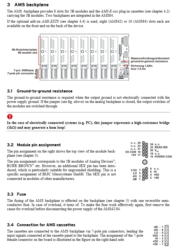
Brand and positioning: The AMS42/84 5B amplifier system, launched by BMCM Messsysteme GMBH, is a modular measurement amplifier designed for industrial measurement scenarios. Its core advantages lie in flexible configuration, channel isolation, and multi signal adaptation. It can be combined with BMCM’s data acquisition (DAQ) cards/systems to form high-performance measurement solutions.
Version differentiation:
|Version | Form Design | Core Features | Number of Basic Channels | Size (W × H × D)|
|AMS42 | Portable, aluminum shell+anti slip foldable foot pad | Mobile use, suitable for desktop scenes | 8-way | 23.5 × 13.2 × 25.6cm|
Power supply specifications: Input 9-40V DC (± 5%), connected through a 3-pole DIN plug, optional accessory ZU-PW70W power supply (24V DC, 2.92A); The minimum power consumption is 3W, and the maximum is 20W (depending on the number of 5B modules installed).
Signal output interface: D-Sub37 female head, which leads the amplified analog signal to the DAQ system. The pin allocation is as follows:
|Pin Range | AMS42 Allocation | AMS84 Allocation|
|1-8 | Analog Output 1-8 | Analog Output 1-8|
|9-16 | Not used (n.c.) | Analog output 9-16|
|20-27 | Channel 1-8 Analog Ground (AGND) | Channel 1-8 Analog Ground (AGND)|
|28-35 | Unused (n.c.) | Channels 9-16 Analog Ground (AGND)|
|Other pins | Unused (n.c.) | Unused (n.c.)|
Modular core components
(1) 5B Measurement Module (MA Series): The core functional unit supports measurement and amplification of different signal types. Most modules have inter channel electrical isolation characteristics, and some provide sensor power supply. The output signal is ± 5V or 0-5V. The specific models are as follows:
|Module model | Function description | Key features|
|MA-UNI | Universal amplifier | Electrical isolation, compatible with U, I, R, PT100, DMS, LVDT signals|
|MA-UI | Multi range amplifier | Electrical isolation, adapted to U and I signals|
|MA-U | Voltage measurement amplifier | Electrical isolation, bandwidth 50kHz|
|MA-FU | Frequency/Voltage Converter | Electrical Isolation, Achieving Frequency Signal to Voltage Output|
|MA-DFI | Digital filtering module | Electrical isolation, attenuation slope of 60dB/octave band|
(2) Plug in box body (AMS-K series): used to carry 5B modules, equipped with different types of connectors at the front end, suitable for various sensors/signal access. The specific models are as follows:
|Box model | Function description|
|AMS-K-BIN5 | 5-core binder female head (712 series)|
Channel Expansion: AMS-EXT8, each device can expand up to 8 analog channels, AMS42 can expand up to 16 channels, AMS84 can expand up to 32 channels, and the expansion channels are output through the second D-Sub37 female head on the back (pin allocation is consistent with the main interface).
Portable accessories: AMS-ANDLE (single-sided folding handle), AMS-ANDLE2 (metal handles on both sides of the body).
Others: USB extension cable (ZUKA-USB), 3-pole DIN female head (ZU3DIN), etc.
Key technical parameters and environmental adaptation
Category specific parameters
Temperature range: -25~50 ℃; Storage: -25~70 ℃
Relative humidity 0~90% (no condensation)
Protection level IP20
Maximum allowable potential 60V DC (compliant with VDE standards)
EMC standards EN61000-6-1, EN61000-6-3, EN61010-1
Compliance with RoHS and WEEE (registration number DE75472248)
Integrated 1.6A reversible semiconductor fuse on the fuse backplate (power off after overload, restart and restore after troubleshooting)
Installation and usage specifications
Installation steps:
a) Assembly plug-in box body: Push the AMS-K series box body equipped with 5B module along the slot guide rail to ensure that the 7-pin connector is docked with the equipment backplane; Unused slots need to be sealed with AMS-K-LANK blank panels.
b) Expansion module installation (if using AMS-EXT8): Install the expansion box on the back of the device.
c) Power connection: Connect 9-40V DC power supply through a 3-pole DIN plug (cable cross-sectional area should be>1mm ²), press the switch to “1” (ON) to start, and the green “ON” LED indicator light will light up to indicate normal operation.
d) Docking with DAQ system: Connect to PC or BMCM DAQ system through D-Sub37 female connector.
e) Signal access: Connect the target signal (such as thermocouple, voltage signal, etc.) to the front connector of the plug-in box.
Important Instructions for Use:
Safety requirements: Only applicable to ultra-low voltage scenarios; CE certified isolated power supply must be used; Signal cables need to use shielded wires, with only one end of the shielding layer grounded; Avoid solvent based cleaning agents and only use non solvent cleaning agents for wiping.
Operation taboos: Before replacing the box, the power must be turned off; Not suitable for security related tasks; Unauthorized modifications will void the warranty.
Maintenance and disposal: The equipment is designed to be maintenance free, and calibration needs to be returned to the BMCM factory; When disposing, it must comply with the WEEE directive and cannot be mixed with household waste.
Core positioning: A fully managed modular Ethernet switch designed specifically for the power industry (substations, distribution networks, and in plant communication), focusing on core requirements such as high reliability, electromagnetic interference resistance, and wide temperature operation in power scenarios, supporting the expansion of smart grid applications (such as renewable energy integration and distribution automation).
Product series division:
|Model series | Installation method | Core configuration differences | Number of ports | Power consumption range | Special functions|
|AFS650/655 | DIN rail (optional wall mounted) | Compact design, supports multi-mode/single-mode optical ports | Up to 10 (including 3 GbE ports) | 12-21 W | Redundant power supply (18-60VDC/48-320VDC/90-265VAC)|
|AFS670/675 | 19 inch rack | Modular design, 12 slots (2 ports/module) | Up to 28 slots (electrical/optical/SFP cage) | 10-40 W (no PoE) | Supports PoE (power type H/Z), redundant power supply (18-60VDC/77-300VDC/90-265VAC)|
|AFS677/AFR677 | 19 inch rack | Fixed port design | 16 GbE combo ports (RJ45/SFP) | 10-40 W (no PoE) | AFR677 supports L3 routing (RIPv1/v2, OSPFv2, VRRP)|
Working temperature: Standard 0-60 ℃, optional -40 ℃ to 85 ℃ (continuous operation)
Switching characteristics: Store and forward mode, typical switching delay of 2.7 μ s (100Mbit/s), MAC address table capacity of 8000 entries
Network function: 4042 VLANs (supporting 255 at the same time), 4 priority queues, supporting port rate limitation (kbps step), link aggregation IGMP snooping
Protection mechanism: Supports RSTP (IEEE802.1D), MRP (IEC62439), E-MRP, and fast switching of ring topology
Power specifications: AFS650/655 supports 18-60VDC (low voltage), 48-320VDC/90-265VAC (high voltage); The AFS670 series supports 18-60VDC (low voltage), 77-300VDC/90-265VAC (high voltage), all of which support redundant power supplies
Substation automation low latency, high availability, IEC61850 compatibility, anti electromagnetic interference pure L2 switching network, redundant topology, multi-mode optical ports as the main, QoS/VLAN enabled, SNMP management supported, GOOSE message and sampling value transmission supported
Long distance transmission of power distribution communication, reliable transmission of SCADA data, multi service carrying FE/GbE backbone network, single-mode optical port (uplink), supporting IEC60870-5-104 protocol, redundant topology+MRP/E-MRP, compatible with VoIP and renewable energy data transmission
In plant communication with high bandwidth (CCTV), equipment power supply, time synchronization, high security GbE upstream connection server, PoE power supply (camera), 802.1x port authentication, SNTP time synchronization, port rate control, supporting CCTV, access control, and public address system communication
Security and management features
Security features: IEEE802.1x port authentication, SSH encryption, Radius centralized password management, multi-level user passwords, port disabling, SNMPv3 encryption authentication, VLAN isolation (IEEE802.1Q)
Management methods: SNMP V1/V2/V3, command-line interface (Telnet), web interface, port mirroring, RMON remote monitoring, LLDP topology auto discovery, SFP diagnosis, configuration recovery adapter (CRA), watchdog and rollback function
Alarm mechanism: Diagnostic LED indicator light, 2 sets of alarm contacts, local logs and Syslog reports
Customer Core Value
Power level adaptation: high EMC/EMI anti-interference ability, wide temperature working range, redundant power supply, suitable for harsh environments in substations
High availability: fanless design, high MTBF, fast switching of link failures, ensuring uninterrupted critical business operations
Flexible Expansion: Port density can be expanded (8-28), supporting FE/GbE, PoE, L3 routing (AFR677), and adapting to different scale requirements
Integrated solution: integrated into ABB’s power communication ecosystem, supporting multi business integration such as SCADA, IEC61850, voice, etc
Key issues
Question 1: What are the specific power level characteristics of ABB AFS series switches reflected in? Why can it adapt to the harsh environment of substations?
Answer: The power level characteristics are mainly reflected in three aspects: ① Environmental adaptation: supporting standard working temperature of 0-60 ℃, optional wide temperature range of -40 ℃ to 85 ℃, fanless design+optional normal coating, and can withstand extreme temperatures; ② Anti interference capability: certified by IEEE1613, compliant with EN61000-4 series (ESD 8kV contact/15kV air discharge, surge 2kV line to ground) and IEEE C37.90 series standards, resistant to strong electromagnetic interference; ③ Reliability design: Supports redundant power supply (AC/DC wide voltage input, such as AFS650 supporting 48-320VDC), fast protection mechanism (MRP/E-MRP, ring topology fast switching), high MTBF guarantee, avoiding single point failure. These characteristics enable it to directly adapt to harsh environments such as severe electromagnetic pollution, large temperature fluctuations, and high requirements for continuity in substations.
Question 2: What are the core differences between different models of ABB AFS series? How to choose the appropriate model based on the application scenario?
Answer: The core differences are concentrated in three dimensions: installation method, port configuration, and functional expansion. The selection logic is as follows:
Model Series Core Differences Adaptation Scenarios
AFS650/655 DIN rail installation, up to 10 ports, no L3 routing for small substations, distribution terminals, and distributed equipment communication within the factory (limited space, low port requirements)
AFS670/675 19 inch rack, modular design (up to 28 ports), supporting PoE for large-scale substation automation, requiring high port density distribution communication backbone network (multi device access, requiring PoE power supply for cameras/terminals)
AFS677/AFR677 19 inch rack, 16 GbE combo ports, AFR677 supports L3 routing (RIPv1/v2, OSPFv2) for cross regional power distribution communication and complex networks requiring routing functionality (multi subnet interconnection, backbone network hierarchical architecture)
Question 3: What are the key technical measures for ABB AFS series switches to ensure the reliability of critical business in the power industry, such as IEC61850 data transmission?
Answer: Key technical measures include: ① Fast protection mechanism: supporting MRP (Media Redundancy Protocol), E-MRP, and RSTP, which can achieve fast switching in case of link failure in ring topology, reducing the interruption time of IEC61850 GOOSE message and sampling value transmission; ② Network isolation and priority: Supports 4042 VLANs (255 at the same time) and 4 priority queues, isolates different services through IEEE802.1Q VLANs, ensures QoS guarantees priority transmission of IEC61850 critical data, and avoids bandwidth preemption; ③ Hardware redundancy: supports redundant power input to avoid equipment shutdown caused by power failure; ④ Management and monitoring: Real time monitoring of network status through SNMP V3, RMON, LLDP topology discovery, combined with alarm contacts and Syslog reports, to quickly locate faults; ⑤ Protocol compatibility: Native support for IEC61850 protocol ensures seamless integration with intelligent electronic devices (IEDs), reducing latency and fault risks caused by protocol conversion
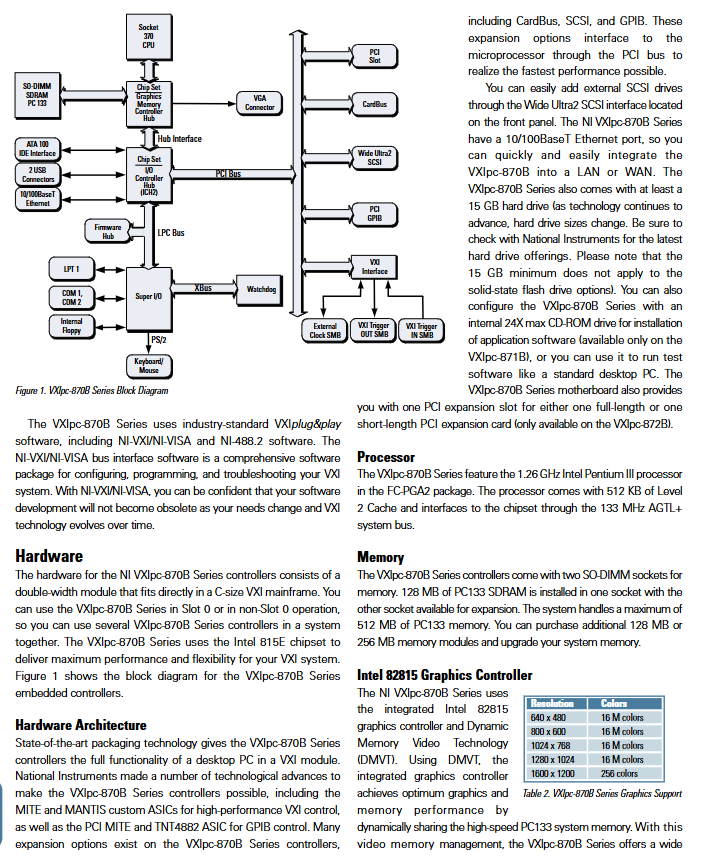
Product Name: NI VXIpc-870B Series Embedded Pentium III VXI Bus Controller
Core advantages: Combining desktop PC full functionality with VXI system specific control capabilities, sturdy structure, suitable for harsh environments, providing cost-effective VXI embedded control solutions
Model differentiation:
Model Core Differences Applicable Scenarios
Scenario where VXIpc-871B integrates 24X max CD-ROM drive and requires on-site installation/operation of application software
VXIpc-872B is equipped with one PCI expansion slot (supporting full-size/short size cards) for scenarios where third-party PCI peripherals need to be expanded
Memory: 128MB PC133 SDRAM (2 SO-DIMM slots, upgradable up to 512MB, supports 128MB/256MB expansion modules)
Storage:
Basic configuration: Internal 1.44MB floppy disk drive+minimum 15GB hard disk (hard disk specifications are subject to technical updates, please consult the manufacturer)
Optional configurations: internal IDE solid state drive, front mounted pluggable ATA solid state drive (replacing hard drives, suitable for harsh environments)
Display and Interface
Display: Intel 82815 integrated graphics card (DMVT technology, dynamic shared system memory), supports the following resolutions and colors:
Maximum number of colors in resolution
640×480 16 million colors
800×600 with 16 million colors
1024×768 with 16 million colors
1280×1024 16 million colors
1600×1200 256 colors
Key interfaces:
Network: 10/100BaseT Ethernet (RJ45, auto negotiate rate)
Storage Expansion: Wide Ultra2 SCSI (LVD/SE mode, 40Mtransfers/s transfer rate, compatible with single ended devices)
Instrument control: GPIB (IEEE 488.2, 26 pin micro interface, supports HS488 protocol, speed up to 8Mbytes/s)
Other interfaces: 2 RS-232 serial ports, 1 IEEE 1284 parallel port, 2 PS/2 interfaces (keyboard/mouse), 2 USB 1.1 interfaces (only supported by Windows 2000), 2 PC Card slots (2 Type I/II or 1 Type III, only supported by Windows 2000)
VXI bus core functions
Address access: Customize ASIC through MITE/MANTIS, support multi window address mapping (3 user configurable windows), covering the entire VXI address space
Data transfer: MITE integrates 2 DMA controllers, supports block mode transfer, and frees up CPU resources
Slot 0 Function: Complete Slot 0 resource management (including MODID register, CLK10 clock source), supports automatic switching between Slot 0 and non Slot 0 (without jumper configuration)
Synchronization and triggering: Front end SMB interface (external CLK10 synchronization, 2 trigger I/O), supporting TTL/ECL trigger lines, event counting, pulse generation, etc
Interrupt handling: Supports all interrupt lines of VXI bus, configurable interrupt assertion and processing priority
Software and Compatibility
Supporting operating systems: Windows 2000, Windows NT, VxWorks, Linux 2.2/2.4 kernel (some features such as USB are only supported by Windows 2000)
Core software: NI-VXI/NI-VISA (compatible with VXIplug&play specifications, supporting various programming environments such as LabVIEW and Visual C++), NI-488.2 (GPIB device control)
Typical total power requirement is 52.4W (+5V: 9.75A;+12V: 150mA; -12V: 50mA, etc.)
Working environment temperature 5-50 ℃, humidity 10% -90% (non condensing)
Storage environment temperature -20-70 ℃, humidity 5% -95% (non condensing)
Reliability meets Bellcore reliability standards, with resistance to impact (30g peak) and vibration (0.3g rms for operation, 2.4g rms for non operation)
Safety certification EN 61010-1, IEC 61010-1
Ordering and Accessories
Basic model code:
Model configuration code
VXIpc-871B without operating system+hard drive 778295-00
VXIpc-871B Windows 2000+hard drive 778295-01
VXIpc-871B Windows NT 4.0+Hard Disk 778295-02
VXIpc-872B without operating system+hard drive 778296-00
VXIpc-872B Windows 2000+hard drive 778296-01
VXIpc-872B Windows NT 4.0+hard drive 778296-02
Optional accessories: Linux/VxWorks specific NI-VXI/NI-VISA software, memory expansion module, solid-state drive, USB CD-ROM drive (compatible only with VXIpc-872B)
Standard accessories: 6-inch parallel port adapter cable, 2-meter GPIB adapter cable, 8-inch serial port adapter cable
BENDER ISOMETER ® The IRDH265/365 series is an insulation monitoring device developed by Bender, a German company, specifically for IT AC systems, IT AC systems with directly connected DC circuits, and IT DC systems (isolated power supplies). Its core mission is to monitor the insulation resistance status between system conductors and the earth (PE) in real time, and to provide timely warning of insulation faults through a graded alarm mechanism, ensuring the safe and stable operation of electrical systems under complex working conditions. This series of products, with patented measurement technology, flexible adaptability, and comprehensive functional configuration, are widely used in industrial scenarios containing rectifiers, converters, thyristor controlled DC drivers, and other components. They fully comply with multiple international universal standards and have high reliability and strong compatibility.
The series includes two core models: IRDH265 (standard plastic housing, supporting DIN rail installation or screw installation) and IRDH365 (embedded housing, 144x72mm size, compatible with panel embedded installation). The functional parameters of the two are the same, with only differences in installation methods and mechanical specifications, which can meet the needs of different installation scenarios.
Core adaptation range
(1) System type adaptation
Basic adaptation system: IT communication systems such as 3AC, 3 (N) AC, single-phase AC, etc; Pure IT DC system
Special adaptation system: IT AC system with direct connection to DC circuit (such as AC system with DC load including rectifier, converter, thyristor controlled DC driver, etc.)
Adaptation prerequisite: In the DC circuit directly connected to the AC system, the rectifier needs to carry a load current of>5… 10mA to ensure accurate monitoring of DC circuit insulation faults
(2) Voltage parameter specifications
Rated monitoring voltage: AC 0… 793V (frequency 50… 400Hz, reference to characteristic curve when frequency<50Hz); DC 0… 650V (slightly different sub series, such as -7 series DC maximum 750V, -8 series DC maximum 650V)
Extended monitoring voltage: It can be extended to higher levels through a dedicated coupling device, with specific adaptations as follows:
AGH204S-4: Suitable for AC 0… 1650V (without rectifier), AC 0… 1300V (with rectifier, DC maximum 1840V)
AGH520S: Suitable for AC 0… 7200V
AGH150W-4: Suitable for DC 0… 1760V
Power supply voltage requirements: Provide multi specification power supply adaptation to meet the power supply needs of different scenarios:
Power type, voltage range, applicable model examples
AC power supply 230V (50… 60Hz) IRDH265-4, IRDH365-4
AC power supply 90… 132V IRDH265-413, IRDH365-413
AC power supply 400V IRDH265-415, IRDH365-415
AC power supply 500V IRDH265-416, IRDH365-416
DC power supply 19.2… 84V IRDH265-422, IRDH365-422
DC power supply 77… 286V IRDH265-423, IRDH365-423
DC power supply 10.5… 80V IRDH265-R421, IRDH265-4921
Power protection: The power input terminal should be equipped with a short-circuit protection device according to the IEC 60364-4-473 standard, and it is recommended to use a 6A fuse
Core technology and functional characteristics
(1) Measurement principle (four levels optional to meet different system requirements)
AMP measurement principle (default): Bender’s patented “adaptive measurement pulse” technology superimposes a pulsating AC measurement voltage with a peak value of 27V (positive and negative pulse amplitudes are consistent), and the measurement period dynamically adjusts with the system’s leakage capacitance and insulation resistance. It is suitable for AC/DC hybrid systems, especially for complex scenarios containing a large number of DC components, with a maximum measurement current of 230 μ A.
DC measurement principle: Overlay 27V DC measurement voltage, only applicable to pure AC systems, insufficient sensitivity for DC insulation fault monitoring, not recommended for use in hybrid systems.
UG/AMP measurement principle: Passive asymmetric measurement (without DC measurement voltage), only applicable to pure DC systems. Fast response is achieved by detecting the DC current and residual voltage generated by L+/L – asymmetric faults. After the alarm is triggered, it automatically switches to the AMP principle to measure insulation resistance. AMP measurement is performed every hour to detect symmetric faults.
AMP/UG measurement principle: AMP measurement is combined with asymmetric measurement. The faults detected by AMP principle are fed back through ALARM2, while those detected by asymmetric measurement are fed back through ALARM1. It is suitable for scenarios that require differentiation of different fault types.
(2) Basic core functions
Insulation monitoring and graded alarm:
Dual level adjustable response values: -3 series 40k Ω/10k Ω, -4 series 180k Ω/40k Ω, -7 series 600k Ω/300k Ω, -8 series 1M Ω/500k Ω (all factory default, adjustable through menu, -3/-4 series adjustment range 10k Ω… 990k Ω), with a hysteresis of approximately 25%.
Fault type differentiation: Supports identification of AC faults and DC faults (including L+/L – single pole faults), and alarm triggering conditions can be set through the Setup 2 menu (only AC, only DC, both AC/DC triggered, etc.).
Alarm output: 2 conversion contact relays, supporting N/O (default) or N/C operation modes, rated contact voltage AC 250V/DC 300V, maximum switching current 5A, adjustable flashing function (1Hz pulse frequency).
Alarm indication: Two yellow alarm LEDs (ALARM1/ALARM2), corresponding to two levels of alarms, will light up intuitively when there is a fault.
Automatic adaptation and self-monitoring:
Leakage capacitance adaptation: The -3/-4 series can adapt to a maximum of 500 μ F, while the -7/-8 series can adapt to a maximum of 2 μ F. The equipment automatically adapts to changes in system leakage capacitance without affecting measurement accuracy.
Automatic self-test: The -3/-4 series automatically performs a self-test every 24 hours (with the alarm relay set to system fault alarm mode), triggered when the insulation resistance exceeds 20 times the maximum response value.
Manual self-test: Press and hold the TEST button (>2s) to start. When there are no faults, it displays “TEST OK R<1k Ω”, the alarm relay acts, and the LED lights up; When a fault is detected, it displays “TEST ALARM”. Press the RESET button (<1s) to clear the fault indication.
Connection monitoring: The -3/-4 series comes standard with a connection monitoring function that continuously monitors the connection status between the device and the IT system or PE. When there is a disconnection or high resistance, it displays “ALARM E-KE” (PE connection fault) or “ALARM L1-L3” (system connection fault), which can be turned off in the Setup 2 menu (recommended for new or small systems).
Display and operation:
Display configuration: LCD display screen, supporting the display of measurement values (unit k Ω/M Ω), response values, fault types (R=AC fault, R+=L+fault, R -=L – fault), menu parameters, etc.
Operation buttons: Both IRDH265/365 are equipped with function buttons (parameter adjustment, menu switching) and a combination TEST/RESET button (short press reset, long press test), supporting external test/reset buttons (cable length ≤ 10m).
Parameter storage: Set parameters to be stored in non-volatile memory (EEPROM) without loss during power failure; Short circuiting the LT terminal can store fault indications, and no faults are stored when the terminal is disconnected.
(3) Extended functions (configured through the Setup 2/Setup 3 menu)
Menu grading configuration:
Setup 1 (basic function): Set alarm response values, relay operation modes (N/O/N/C), password query, jump to Setup 2.
Setup 2 (Extended Function): Configure alarm fault types, coupling device parameters, connection monitoring switches, alarm flashing function, relay test switches, alarm time delay (1… 10s), maximum leakage capacitance matching, password activation and modification, restore factory settings, and view software versions.
Setup 3 (Measurement Principle): Select the measurement principle (AMP/DC/UG/AMP/AMP/UG) and set the DC fast response current level (0.1… 5mA).
Password Protection: Supports activating a two letter password to prevent unauthorized modification of parameters. Passwords can be set and reset in the Setup 2 menu.
System fault handling: When the LCD displays “TEST ALARM”, the device needs to be powered off for a moment before restarting. If the fault still exists, it is highly likely to be a fault of the device itself and requires maintenance.
Status word display: Press and hold the IRDH265 function key for ≥ 5 seconds to display the status word, which includes key configuration information such as relay mode, alarm function, connection monitoring status, measurement principle, etc.
(4) Interface and communication functions
RS-485 interface: No electrical isolation, compliant with EIA R5-485 standard, terminal A/B wiring, maximum transmission distance of 1200m, transmission protocol of 9600 Baud (1 start bit+8 data bits+1 stop bit), continuous transmission of measurement values, alarm status and other data blocks, cannot be interrupted by other bus members.
External indication interface: The M+/M – terminal supports external k Ω measuring instruments (0… 400 μ A analog output), and this interface has no electrical isolation. When connecting to the process control system, an additional isolation module (such as RK170) needs to be configured.
Mechanical specifications and environmental adaptability
Installation note: Only one active ISOMETER is allowed to be connected to each interconnected system in the IT system ®; Terminals E and KE need to be connected to PE through separate wires, and this connection cannot be disconnected during equipment operation; The installation distance between adjacent devices should be ≥ 10mm (ventilation gap should be reserved when the temperature is>40 ℃).
Storage temperature: -40…+70 ℃ (standard version), -45…+85 ℃ (T-option version), display screen function is only guaranteed above -40 ℃
Climate grade: IEC 60721-3-3 3K5 (no condensation, no icing)
Anti interference performance: compliant with EN 50082-2 (anti electromagnetic interference), EN 55011/CISPR11 (electromagnetic emission, Class A, Suitable for industrial scenarios)
Mechanical anti-interference: anti impact 15g/11ms (standard version), 30g/11ms (T-option version); Anti collision 40g/6ms; Anti vibration 10… 150Hz/0.15mm-2g (standard version), 1.6mm/10-25Hz+4g/25… 150Hz (T-option version)
BENDER ISOMETER ® The IRDH375 series is an insulation monitoring device developed by Bender, a German company, specifically for ungrounded alternating current (AC), mixed AC/DC, and direct current (DC) systems (i.e. IT systems). Its core mission is to monitor the insulation resistance status between the system conductor and the ground in real time, warn of insulation faults in a timely manner, and ensure the safe and stable operation of electrical systems. This series of products, with patented measurement technology, flexible adaptability, and comprehensive functional configuration, are widely used in various scenarios with strict electrical safety requirements, and fully comply with multiple international universal standards, possessing high reliability and compatibility.
Core adaptation range
(1) System type adaptation
Basic adaptation systems: AC system, DC system, AC/DC hybrid main circuit
Special adaptation system: AC/DC main circuit with direct connection to DC components (such as rectifiers, converters, thyristor controlled DC drivers); UPS system, battery system; Phase controlled heater; Installation scenarios for equipment with switch mode power supply; High leakage capacitance IT system; Coupling IT systems
(2) Voltage parameter specifications
Rated monitoring voltage: AC/AC-DC 0… 793V, DC 0… 650V
Extended monitoring voltage: By combining with a dedicated coupling device, it can be extended to higher voltage levels such as DC 0… 1760V, 3/(N)/AC 0… 7200V (50… 400Hz), etc
Power supply voltage requirements:
AC power supply: 88… 264V (frequency 42… 460Hz)
DC power supply: 77… 286V or 19.2… 72V (please refer to the equipment nameplate for details)
Power protection: requires power supply through a 6A fuse; Mandatory requirement to use 5A fuses for UL and CSA application scenarios
Core technology and functional characteristics
(1) Measurement technology
Adopting the patented AMPPlus measurement method, designed specifically for modern power supply systems, it can accurately respond to complex scenarios containing a large number of directly connected DC components and high system leakage capacitors, effectively solving the problem of inaccurate monitoring by traditional measurement methods in such scenarios, and ensuring the stability and reliability of insulation resistance monitoring.
(2) Basic functions
Insulation monitoring core: Real time monitoring system insulation resistance, supporting two independent adjustable response values (1k Ω… 10M Ω), can set warning threshold and alarm threshold separately, achieving graded warning
Automatic adaptation capability: Without manual intervention, the device can automatically adapt to system leakage capacitance (maximum allowable value ≤ 500 μ F) and adapt to changes in system parameters under different operating conditions
Self monitoring and self testing:
Continuous self-monitoring: Real time inspection of the device’s own working status, automatic triggering of system fault alarm in case of malfunction
Optional automatic self testing: supports manual self testing through the TEST button to verify device functionality and the connection status between the system and the earth
Display and operation:
Display configuration: Dual row backlit LCD display screen, supports switching between standard mode and menu mode, clearly displays insulation resistance value, device settings, fault information, etc
Operation buttons: equipped with four core buttons: INFO (query standard information), TEST (self-test), RESET (clear fault alarm), MENU (activate menu system), and support direction keys (up/down) and confirm key operation. Parameter configuration can be completed through panel buttons; Support external testing and reset buttons (cable length ≤ 10m)
Alarm function:
Alarm output: 2 independent alarm relays, both with passive conversion contacts, supporting N/O (normally open) or N/C (normally closed) operation modes; Additional configuration of system fault alarm relay (default N/C operation mode)
Alarm indication: 3 dedicated alarm LED lights, corresponding to “Level 1 Insulation Fault Warning”, “Level 2 Insulation Fault Alarm”, and “Equipment Self Fault”, providing intuitive feedback on the alarm level
Fault storage: It can store fault information and clear it through the RESET button or external reset button (when terminals R1/R2 are disconnected and the storage function is not activated through the operation menu, the fault information is not stored)
Extension interface:
Communication interface: RS-485 interface (supports ASCII protocol), transmission distance ≤ 1200m (recommended to use J-Y (St) Y 2 × 0.8mm ² twisted pair, with one end of the shielding layer connected to PE), supports communication with external systems
External indicator interface: Reserve an external k Ω indicator interface (output 0… 400 μ A signal), which can be connected to external measuring instruments to display insulation resistance values
Terminal design: adopting plug-in terminals, convenient wiring, and terminal protection level up to IP30
Other auxiliary functions:
INFO button: Press to query additional information such as system leakage capacitance, current device settings, etc
Standby function: Controlled through function input ports F1 and F2, the device enters standby mode when the contacts are closed, pausing insulation measurement and achieving system disconnection control
DIP switch configuration: When the S1 switch is in the “ON” state, the RS-485 interface enables a 120 Ω terminal resistor; S2 switch has not yet been assigned a function
(3) Advanced features of IRDH375B (added compared to the base model)
Historical record storage: Built in historical memory with real-time clock, which can record all alarm information and attach date and time stamps for easy fault tracing and analysis
Enhanced Communication Capability: Equipped with an electrically isolated RS-485 interface, supporting BMS protocol, capable of stable communication with other Bender devices, and adaptable to centralized control scenarios such as building management systems
Coupling system adaptation: Built in insulation monitoring device disconnect relay, supports multiple IRDH375B devices to work together in the coupling IT system, and ensures that only one device is active at any time by controlling input ports F1/F2 to avoid monitoring conflicts
Analog output: Added 0 (4)… 20mA current output, which can be used for external data acquisition devices to achieve remote transmission and recording of insulation resistance data
Key performance parameters
Specific parameter specifications for performance categories
When the insulation resistance R_F=0.5 x the set response value R_an and the system leakage capacitance C_e=1 μ F, the response time is ≤ 5s
Anti interference and mechanical performance electromagnetic compatibility (EMC): compliant with IEC 61326-2-4:2006-06 Ed.1.0 standard; Impact resistance: IEC 60068-2-27 (15g/11ms); Anti collision (transportation): IEC 60068-2-29 (40g/6ms); Vibration resistance: IEC 60068-2-6 (1g/10… 150Hz, transportation scenario 2g/10… 150Hz); Option-W enhances impact resistance (30g/11ms) and vibration resistance (1.6mm/10-25Hz, 4g/25… 150Hz) performance
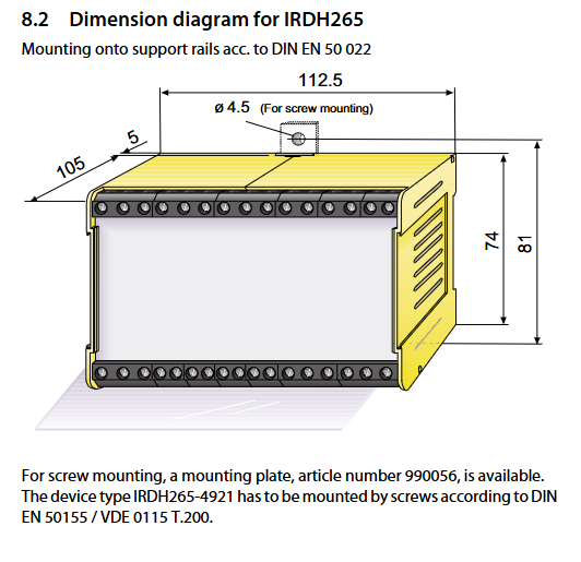
Mechanical specification panel opening size: 138 × 68mm; installation method: DIN rail installation (in accordance with IEC 60715 standard) or screw installation (2 × M4); Shell type: X300 type, halogen-free material; Protection level: IP20 for equipment casing; Weight ≤ 510g; distance between adjacent equipment installations ≥ 30mm
Wiring specification terminal type: spiral terminal; Conductor adaptation: rigid conductor 0.2… 4mm ², flexible conductor (with/without plastic sleeve) 0.2… 2.5mm ²; Suitable for AWG wire gauge: 24… 12; Terminal pairs 10, 11, and 12 must be electrically isolated and must not be connected to PE
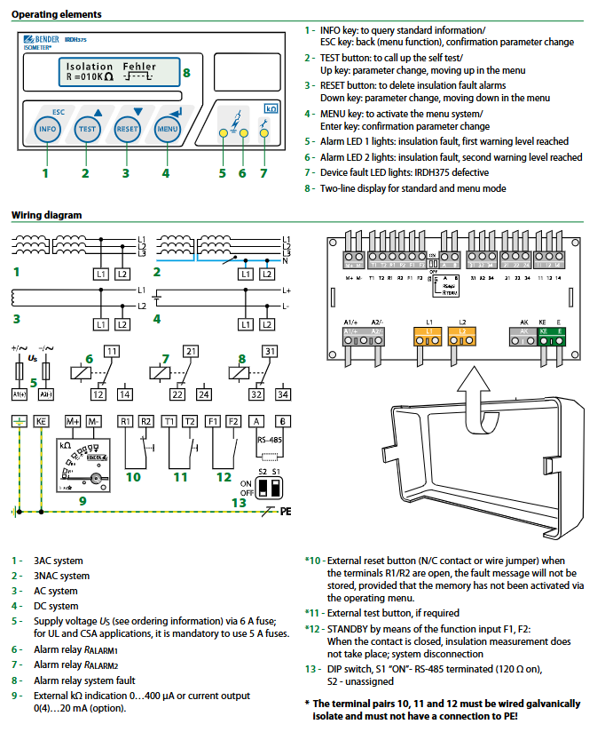
Operation and Display Instructions
(1) Operation button function
Core functions of buttons/operating components
INFO key to query standard information; Cooperate with menu operations to achieve function switching
Return to the previous level in ESC menu mode; Confirm parameter changes
Test button to start device self-test; As an up arrow key in menu mode, it is used for parameter changes and menu navigation
The RESET button clears the insulation fault alarm record; As the down arrow key in menu mode, it is used for parameter changes and menu navigation
MENU key activates the menu system; As a confirmation key in menu mode, confirm parameter changes
Alarm LED 1 lights up to indicate insulation fault, reaching the first level warning threshold
Alarm LED 2 lights up to indicate insulation fault, reaching the second level alarm threshold
Device fault LED lights up to indicate a device malfunction (IRDH375 malfunction)
Dual row display screen standard mode displays insulation resistance value and fault information; Menu mode displays parameter configuration interface
(2) Parameter configuration method
Support two parameter configuration methods: one is to operate through the dual row LCD display screen on the device panel in conjunction with functional buttons; The second is to connect to the external control system through the RS-485 interface for remote configuration (in accordance with the corresponding communication protocol). During the configuration process, changes can be confirmed through the ESC key or Enter key, and the operation logic is clear and easy to understand.
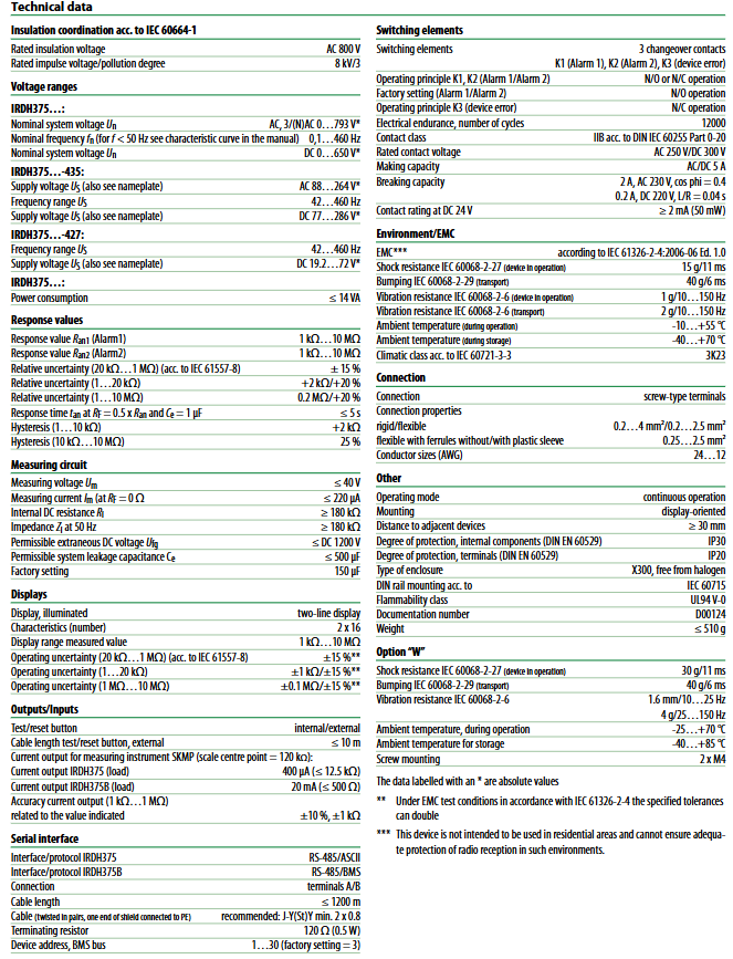
WR70x175S (P)… WR200x500S (P) is an industrial grade rectangular measuring current transformer developed by BENDER in Germany. It is designed for current signal conversion and precise acquisition, and is used in conjunction with residual current monitoring systems and insulation fault location systems to achieve current monitoring and fault tracing in industrial electrical circuits. It is suitable for AC/DC hybrid power supply scenarios and can convert high or positioning currents on the primary side into assessable standard signals on the secondary side, providing accurate data support for backend monitoring equipment. It is widely used in industrial scenarios such as factory distribution systems, busbar systems, IT systems (ungrounded systems), etc.
(2) Core Features and Compliance Standards
1. Core Features
Dual scenario adaptation: compatible with RCM/RCMS series residual current monitoring systems, converting AC current signals; It can also be paired with EDS series insulation fault location system (IT system) to collect the positioning current generated by PGH positioning current injector or IRDH series insulation monitoring instrument.
Series differentiation design: divided into the S series without integrated shielding and the SP series with integrated shielding. The SP series is designed specifically for busbar systems with load currents ≥ 500A, which can avoid false triggering of backend devices caused by high load currents or surge currents.
High reliability: Equipped with a built-in secondary side overvoltage protection diode, it has strong resistance to impact and vibration, and is suitable for harsh industrial environments.
Flexible installation: Supports installation in any direction, adapts wires to multiple specifications, and meets different on-site wiring needs.
2. Compliance and Certification
Following standards: DIN EN 60044-1 (General Technical Standard for Current Transformers), IEC 61869 (Power Transformer Standard), IEC 61869-2 (Insulation Coordination Standard), DIN IEC 60721-3-3 (Climate Rating Standard).
Safety level: The flame retardant rating of the shell reaches UL94 V-0, the internal component protection level is IP40, and the terminal protection level is IP20, effectively preventing solid foreign objects from entering and electrical safety risks.
Product classification and core parameters
(1) Product series and model differentiation
Series Core Features Applicable Scenarios Model Range
S series without integrated shielding, basic design for conventional industrial scenarios, circuits with load current<500A WR70x175S、WR115x305S、WR150x350S、WR200x500S
SP series with integrated shielding, strong anti-interference ability, busbar system, circuit with load current ≥ 500A, high interference environment WR70x175SP, WR115x305SP, WR150x350SP, WR200x500SP
(2) Key electrical parameters
Category specific specification remarks
Maximum system voltage (Um) AC 720 V suitable for medium and high voltage industrial distribution systems
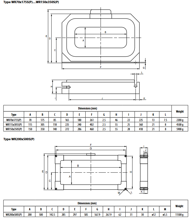
It is strictly prohibited to pass shielded cables, PE conductors, and low resistance conductor circuits through transformers, otherwise interference signals may be introduced, leading to a decrease in measurement accuracy or misjudgment by backend equipment.
All current carrying wires must pass through the transformer completely without omission, ensuring comprehensive collection of current signals.
Wire threading direction and position:
The wire needs to be threaded in from the P1 (K end, yellow mark) side and out from the P2 (L end, gray mark) side. Incorrect direction can cause signal polarity reversal and affect data accuracy.
The wires need to be aligned with the center position of the transformer to avoid uneven magnetic field distribution caused by offset, further ensuring measurement accuracy.
Wire bending and spacing:
The bending of the primary side conductor must follow the minimum bending radius specified by the manufacturer, and the 90 ° bending distance must not be less than twice the height of the transformer to prevent insulation damage to the conductor and distortion of current distribution.
Installation and fixation:
Supports installation in any direction (horizontal, vertical, etc.), fixed on the installation surface with M5 screws to ensure a firm and secure installation without looseness, and to avoid vibration affecting performance during operation.
(2) Wiring and Connection Specifications
Conductor adaptation:
The terminal block is screw type and supports rigid conductors (0.2… 4mm ²), flexible conductors (0.2… 2.5mm ²), and flexible conductors with/without plastic collars (0.25… 2.5mm ²), compatible with AWG 24… 12 specification conductors.
Cable selection and distance:
Single core wire (≥ 0.75mm ²): maximum connection distance of 1m.
Twisted single core wire (≥ 0.75mm ²): maximum connection distance of 10m.
Shielded cable (≥ 0.6mm ²): maximum connection distance of 40m, recommended model J-Y (St) Y 2 × 0.6mm ², shielding layer needs to be connected to PE at one end to reduce electromagnetic interference.
Wiring precautions:
Before wiring, the power supply must be disconnected to ensure construction safety; Tighten the terminal screws after wiring to avoid signal distortion caused by poor contact.
Connected to backend devices (RCM/RCMS/EDS) through two-wire cables, S1 (k) and S2 (l) terminals correspond to device signal input interfaces.
Environmental adaptability and mechanical characteristics
(1) Environmental parameters
Category specific specifications
Working environment temperature -10 ℃…+50 ℃
Storage environment temperature -40 ℃…+70 ℃
Climate grade DIN IEC 60721-3-3 (3K22)
Impact resistance performance (in operation) 15 g/11 ms (IEC 60068-2-27)
Anti collision performance (during transportation) 40 g/6 ms (IEC 60068-2-29)
Selection based on load current: If the load current is ≥ 500A or applied to the busbar system, the SP series (with shielding) is preferred; For conventional load current scenarios, select the S series.
Select according to internal dimensions: Select the corresponding internal dimensions based on the number and thickness of the primary side conductors to ensure that the conductors can pass through the transformer smoothly and leave appropriate gaps.
Selection based on connection distance: When the connection distance exceeds 10m, shielded cables should be selected and matched with the wiring requirements of the corresponding transformer model.
Precautions and Maintenance Guidelines
(1) Precautions for use
It is strictly prohibited to dismantle the transformer casing or modify the internal circuit without authorization, otherwise it will damage the insulation performance and shielding structure, and lose the product warranty qualification.
Transformers need to be used in conjunction with compatible backend devices (RCM/RCMS/EDS) to avoid signal attenuation or equipment damage caused by load mismatch.
Installation and maintenance must be carried out by qualified electrical professionals, strictly following local electrical safety regulations.
(2) Key points of daily maintenance
Regular inspection: Check the installation and fixation of the transformer, whether the wiring terminals are loose, and whether the cable insulation layer is damaged every month. If any problems are found, they should be dealt with in a timely manner.
Environmental cleaning: Keep the surface of the transformer clean to avoid dust accumulation affecting heat dissipation or insulation performance.
Fault handling: If there is no signal input or signal abnormality in the backend equipment, it is necessary to sequentially check whether the cable connection, conductor direction, and transformer are damaged. If necessary, contact the manufacturer’s technical support.
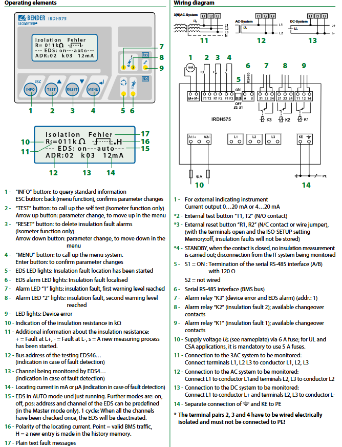
IRDH575 is an industrial grade insulation monitoring and fault location control integrated equipment launched by BENDER in Germany. It is designed specifically for ungrounded (IT) systems and is used to monitor the ground insulation resistance of 3 (N) AC, AC/DC hybrid, and pure DC systems in real time, identify the risk of grounding faults in advance, and can be expanded into an accurate fault location system. It is suitable for industrial scenarios with sensitive loads such as frequency converters, thyristor controlled DC drives, PLCs, etc., such as factory power distribution systems, automated production lines, new energy equipment, etc. Through the dual functions of “monitoring and warning+precise positioning”, it ensures the electrical safety and continuous operation of IT systems, avoiding equipment damage or production interruption caused by grounding faults.
(2) Core Features and Compliance Standards
1. Core Features
Strong universality: It has a wide voltage range of adaptation (AC/DC 20… 575V low voltage type, 340… 760V high voltage type) and is compatible with multiple types of IT systems.
Accurate monitoring: The insulation resistance measurement range is 1k Ω… 10M Ω, supporting two-level alarm thresholds to distinguish between “potential risks” and “serious faults” in advance.
Positioning Expansion: Paired with EDS4 series positioning devices, it can cover up to 1080 circuits and accurately locate fault branches and sources.
Comprehensive functionality: It has multiple functions such as data storage, bidirectional communication, self-monitoring, and external device expansion, and is suitable for industrial centralized monitoring needs.
2. Compliance and Certification
Following standards: DIN EN 61557-8/9(VDE 0413-8/9)、IEC 61557-8/9、IEC 61326-2-4、ASTM F1669M-96(2007)、ASTM F1207M-96(2007)、DIN EN 60664-1/3(VDE 0110-1) Wait.
Certification qualifications: CE, UL/US LISTED certification, the shell adopts halogen-free design, and the flame retardant level reaches UL94 V-0, which meets environmental and safety requirements.
Core functions and operational features
(1) Insulation monitoring function
Core measurement mechanism
Measurement principle: Using the AMP measurement method, a weak test signal (measured voltage ≤ 40V, measured current ≤ 220 µ A) is injected into the system through a built-in measurement circuit to monitor the insulation resistance between the system conductor and ground. The measurement results are not affected by the system load current and rated voltage, and have strong stability.
Measurement range: 1k Ω… 10M Ω, covering the entire scene from low resistance faults (close to short circuits) to high resistance faults (slight insulation damage), and can identify faults in advance before leakage current occurs.
Measurement accuracy: The range error of 10k Ω… 10M Ω is 0%…+20%, and the range error of 1k Ω… 10k Ω is+2k Ω. The measurement data is reliable and provides accurate basis for fault diagnosis.
Hierarchical alarm mechanism
Alarm output: 3 switch contacts (SPDT), corresponding to first level alarm (K1, warning), second level alarm (K2, main alarm), equipment failure/EDS alarm (K3), supporting N/O (normally open) or N/C (normally closed) operation mode switching, factory default K1/K2 is N/O, K3 is N/C.
Alarm mode: Supports self-locking mode (manual reset after fault clearance) and non self-locking mode (automatic reset after fault clearance), which can be switched through menu settings and adapted to different fault handling processes.
Status indication: Alarm LED1 (first level alarm), Alarm LED2 (second level alarm), and equipment fault LED correspond to different alarm levels, providing intuitive feedback on the severity of the fault for quick on-site identification.
Self monitoring and testing
Self monitoring: Continuously monitor the grounding connection, line connection, and internal circuit status of the equipment itself. In case of abnormalities, trigger the K3 relay action and light up the equipment fault LED to avoid missed reports due to equipment failure.
Testing function: Supports internal/external testing buttons (N/O contacts), long press the TEST button to activate self-test, verify whether the alarm circuit, display system, and connection to the system/ground are normal, and ensure reliable device functionality.
Reset function: Internal/external reset button (N/C contact or jumper), short press the RESET button to clear the alarm memory. When the terminal is open and ISO-SETUP is set to Memory: off, insulation faults are not stored.
(2) Ground fault location function
System expansion configuration
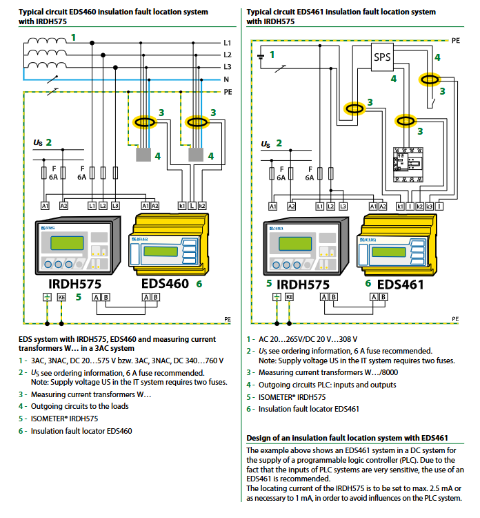
Core components: IRDH575 host+EDS460 (main circuit positioning device)/EDS461 (control circuit positioning device)+dedicated current transformer (W series adapted to main circuit, 8000 series adapted to control circuit), optional EDS3090/EDS3091 portable positioning system.
Scalability: Supports up to 90 EDS4 series devices for interconnection, with each EDS device capable of monitoring 12 circuits, covering a total of 1080 circuits, and adapting to the fault location needs of large industrial distribution systems.
Positioning workflow
Trigger method: After IRDH575 detects an insulation fault, it automatically starts the positioning process, or can be manually started through the menu, flexibly adapting to different on-site requirements.
Signal generation: IRDH575 generates pulse positioning current, the amplitude of which depends on the system voltage and the degree of insulation fault. In case of low resistance fault, the positioning current is automatically limited, and the current limit value can be set through the menu (maximum 50mA). The pulse period is 2s and the interval is 4s to avoid affecting the normal operation of the system.
Fault identification: The positioning current pulse starts from the host through live parts, travels along the shortest path to the fault point, and then returns to the host through the insulation fault point and PE line. The current transformer on the fault path collects the pulse signal, which is evaluated by EDS equipment.
The results show that when the positioning current exceeds the response value of the EDS device, the EDS local alarm LED lights up, indicating the faulty sub circuit. At the same time, the IRDH575 LCD synchronously displays the bus address, monitoring channel, and positioning current intensity (mA/µ A) of the faulty EDS device, achieving accurate fault positioning.
Portable troubleshooting: Optional EDS3090/EDS3091 portable positioning system can track pulse signals to the source of faults, suitable for complex wiring and concealed fault troubleshooting scenarios.
PLC control circuit adaptation
Due to the sensitivity of PLC input signals, EDS461 equipment is required for control circuit positioning, and the positioning current of IRDH575 should be set to a maximum of 2.5mA or 1mA to avoid interfering with the normal operation of the PLC.
(3) Data storage and communication functions
Data recording and querying
Storage capacity: Non volatile memory can store 99 alarm messages with date and timestamp, including fault type, insulation resistance value, occurrence time, EDS device address, etc. Data will not be lost after power failure, making it easy to trace and analyze faults.
Information query: Pressing the INFO key can quickly query system leakage capacitance, device parameter settings, alarm history, and other information without entering deep menus, making operation convenient.
communication interface
RS-485 interface (BMS protocol): Supports bidirectional data communication between devices, with a maximum cable length of 1200m. It is recommended to use shielded cable J-Y (ST) Y 2 × 0.6mm ² (single ended PE for shielding layer), equipped with a 120 Ω terminal resistor (controlled by micro switch S1 to enable/disable), to reduce signal attenuation and electromagnetic interference.
Protocol extension: Can connect to Bendel protocol converters, adapt to industrial protocols such as Ethernet, MODBUS, PROFIBUS, etc., and achieve interconnection with upper control systems such as PLC and DCS.
Analog output: 0/4… 20mA optional, load ≤ 500 Ω, can convert insulation resistance signal into standard analog quantity, connect to external instruments or centralized monitoring system, achieve remote real-time monitoring of insulation status.
(4) Operation and display functions
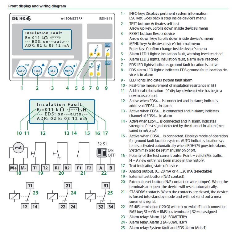
display system
Backlit LCD screen: 4 × 16 character pure text display, character height 5mm, clear display, supports multilingual switching, real-time display of insulation resistance value (k Ω), system status, alarm information, EDS equipment status, etc.
Auxiliary display: “s” indicates that a new measurement is in progress, “+” indicates a fault on the L+side, and “-” indicates a fault on the L – side; EDS mode display (AUTO/ON/OFF/pos/1 cycle), POS mode can preset EDS address and channel (host mode only), EDS will automatically stop after detecting all channels in 1 cycle mode; Position current polarity indication (Point=active BMS communication, H=new historical record).
Operation buttons
Function keys: INFO (information query), MENU (menu call), ESC (return/confirm parameter modification), TEST (self-test), RESET (alarm reset).
Operation logic: Clear menu hierarchy, intuitive parameter settings, password protection support to prevent unauthorized personnel from tampering with settings.
Detailed technical parameters
(1) Electrical parameters
Category specific specifications
Monitoring system voltage low voltage type (B1 series): AC 20… 575V (3 (N) AC/single-phase, 50… 460Hz), DC 20… 575V
High voltage type (B2 series): AC 340… 760V (3 (N) AC/single-phase, 50… 460Hz), DC 340… 575V
Supply voltage AC 88… 264V (50… 460Hz), DC 77… 286V; UL/CSA applications mandate the use of 5A fuses, while 6A fuses are recommended for other scenarios; Two fuses are required for IT system power supply
Allow external DC voltage B1 series ≤ 810V, B2 series ≤ 1060V
Allow system leakage capacitance ≤ 150 (500) µ F
Relay parameters: rated contact voltage AC 250V/DC 300V, connection capacity AC/DC 5A, breaking capacity 2 A(AC 230V,cosφ=0.4)、0.2A(DC 220V,L/R=0.04s), Electrical lifespan of 12000 cycles, contact current (DC 24V) ≥ 2mA (50mW), contact level IIB (DIN IEC 60255-23)
Analog output 0/4… 20mA, load ≤ 500 Ω
Power consumption ≤ 14 VA
(2) Environmental and mechanical parameters
Category specific specifications
Working environment temperature -10 ℃…+55 ℃ (cannot operate continuously in 50mA positioning mode); The short-term working temperature can reach -25 ℃…+70 ℃
Storage environment temperature -40 ℃…+85 ℃
Climate grade DIN IEC 60721-3-3 (3K5)
Impact resistance performance during operation: 15g/11ms (IEC 60068-2-27); During transportation: 40g/6ms (IEC 60068-2-29); Option-W model: 30g/11ms
Shell and weight halogen-free flame-retardant shell, weight ≤ 900g
System installation and typical configuration
(1) Installation points
Power supply configuration: The power supply circuit is connected in series with corresponding specifications of fuses (5A for UL/CSA, 6A for others). The IT system power supply must be equipped with two fuses to ensure equipment overcurrent protection.
Grounding requirements: The equipment grounding terminal (KE) should be reliably grounded, and the RS-485 cable shielding layer should be single ended with PE to reduce electromagnetic interference; Terminal pairs 2, 3, and 4 require electrical isolation wiring and must not be connected to PE.
Wiring specifications: Measurement circuits and power cables should be laid separately to avoid cross interference; The wiring between EDS equipment and current transformers must follow polarity requirements to ensure accurate signal acquisition.
Environmental requirements: The installation location should be well ventilated, away from heat sources and strong electromagnetic interference sources, and meet the working temperature (-10…+55 ℃) and protection level requirements; The Option-W model has stronger shock and vibration resistance and is suitable for harsh environments.
(2) Typical application configuration
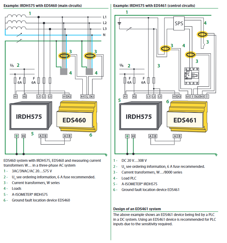
1. Main circuit monitoring and positioning system (AC/DC 20… 575V)
Configuration components: IRDH575B1-435+EDS460+W series current transformer+6A fuse.
Applicable scenarios: Factory three-phase main distribution circuit, motor control circuit, etc. Each EDS460 monitors 12 main circuit branches and supports cascading expansion of multiple EDS460.
Wiring method: The L1/L2/L3 terminals of the 3AC system are respectively connected to the L1/L2/L3 terminals of the equipment, the N line is connected as needed, and the KE terminal of the equipment is connected to PE; EDS460 communicates with IRDH575 through the AB terminal, and the current transformer is installed on the main circuit branch line.
2. Control circuit monitoring and positioning system (AC 20… 265V/DC 20… 308V)
Configuration components: IRDH575B1-435+EDS461+8000 series current transformer+6A fuse+PLC.
Applicable scenarios: PLC control circuits, DC instrument circuits, and other sensitive load circuits. EDS461 is designed to meet the high sensitivity requirements of control circuits and avoid interference from positioning currents on loads.
Wiring method: The L+terminal of the DC system is connected to the L1 terminal of the device, the L – terminal is connected to the L2/L3 terminal, and the KE terminal of the device is connected to the PE terminal. EDS461 communicates with IRDH575, and the current transformer is installed on the PLC input and output circuit line, with a positioning current set to 1… 2.5mA.
Product Name: IRDH575 Digital Ground Fault Monitor/Ground Fault Localization System Controller
Applicable systems: ungrounded (floating) AC/DC systems, including 3 (N) AC, AC/DC hybrid, pure DC systems, suitable for industrial scenarios with power conversion equipment such as rectifiers and frequency converters
Core value: By monitoring the insulation resistance of the system to ground, ground faults can be detected in advance (can be identified when there is no leakage current), which can be expanded into a ground fault location system to accurately locate the fault circuit and ensure the electrical safety of ungrounded systems
Core functions and features
(1) Fault detection and alarm
Insulation resistance monitoring: The core determines faults by measuring the insulation resistance of the system to the ground, with a response range of 1k Ω… 10M Ω. It supports two-level adjustable alarm thresholds (R_an1 warning, R_an2 main alarm) and can distinguish different risk levels.
Hierarchical alarm mechanism:
Dual independent alarm relays (K1, K2), supporting constant power on or constant power-off operation mode, default constant power-off at the factory.
Alarm mode: self-locking mode (manual reset required after fault clearance), non self-locking mode (automatic reset after fault clearance).
Self monitoring function: Continuously monitor the status of the device’s grounding connection and line connection, trigger the system fault alarm relay (K3) in case of abnormalities, and support EDS positioning device alarm linkage.
(2) Grounding fault location
Scalability: Equipped with positioning devices such as EDS460 (main circuit), EDS461 (control circuit), and dedicated current transformers, it can be expanded into a ground fault positioning system, supporting up to 90 EDS4 devices for interconnection. Each EDS device monitors 12 circuits, covering a total of 1080 circuits.
Positioning principle: After detecting a ground fault, IRDH575 sends a pulse test signal (pulse/interval=2s/4s), which returns to the host through the fault circuit. The fault EDS address, circuit number, and signal strength are synchronously displayed on the LCD and EDS equipment.
Portable extension: optional EDS30… portable positioning system, tracks pulse signals to the source of faults, suitable for mobile troubleshooting scenarios.
(3) Data Storage and Communication
Data recording: Non volatile memory can store 99 alarm messages with timestamps, facilitating fault tracing and analysis.
Communication interface:
RS-485 interface (BMS protocol), supports bidirectional communication between devices, can be connected to Bendel protocol converters, and is compatible with Ethernet, MODBUS, PROFIBUS and other protocols.
0/4… 20mA analog output (load ≤ 500 Ω), can be connected to upper control systems such as PLC and DCS to achieve centralized monitoring.
Operation and Display:
Display: Backlit LCD screen (4 × 16 characters, character height 5mm), real-time display of insulation resistance (1k Ω… 10M Ω), system status, EDS equipment information, etc.
Operation: Equipped with INFO (parameter query), MENU (menu settings), ESC (return), TEST (test), RESET (reset) buttons, supporting internal/external test/reset buttons (remote operation).
Detailed technical parameters
(1) Electrical parameters
Category specific specifications
Monitoring system voltage IRDH575B1-435: AC 20… 575V, DC 20… 575V; IRDH575B2-435:AC 340…760V、DC 340…575V
Supply voltage AC 88… 264V (50… 460Hz), DC 77… 286V
Plug in screw terminals for wiring terminals, supporting rigid conductors of 0.2… 4mm ² and flexible conductors of 0.2… 2.5mm ²
Weight ≤ 900 g
(3) Communication parameters
Category specific specifications
Interface type RS-485 (BMS protocol)
Maximum cable length of 1200 meters
Recommended shielded cable J-Y (ST) Y 2 × 0.6mm ² (shielding layer single ended PE)
Terminal resistance of 120 Ω (0.5W), controlled by micro switch S1
System configuration and installation
(1) Typical system composition
Number of component functions/adaptation
IRDH575 host fault detection, alarm control, positioning system management 1 unit/independent system
Up to 90 EDS460 main circuit grounding fault location devices, each with 12 circuits
EDS461 control circuit grounding fault location equipment (adapted to PLC input) up to 90 units, with 12 circuits per unit
Current transformer signal acquisition, compatible with main circuit/control circuit and EDS equipment
EDS30… Portable grounding fault location system optional for mobile troubleshooting
(2) Installation points
It is recommended to connect 6A fuses in series for the power supply circuit, and two fuses are required for IT system power supply.
When wiring, it is necessary to ensure reliable grounding of the equipment. The shielding layer of the RS-485 cable should be connected to PE at one end, and the terminal resistance should be enabled as needed (for long-distance communication).
The installation location should be far away from strong electromagnetic interference sources, ensure good ventilation, and meet the requirements of working temperature and protection level.
Ordering and Accessories
Core models: IRDH575B1-435 (low voltage range), IRDH575B2-435 (high voltage range)
Supporting equipment: EDS460 (main circuit positioning), EDS461 (control circuit positioning), EDS3090/3091 (portable positioning), dedicated current transformers (W series/8000 series)
RCMA475LY is an industrial grade AC/DC sensitive residual current monitor launched by BENDER in Germany, designed specifically for TN and TT systems (grounded power supply systems). Its core function is to monitor AC, DC, and pulsating DC currents in circuits, accurately identify DC fault currents or residual currents that are continuously greater than zero, and prevent safety risks such as electrical fires and electric shocks. Its unique Type B working characteristics make it particularly suitable for scenarios containing six pulse rectifiers, unidirectional rectification filtering loads, such as frequency converters, battery chargers, construction site variable frequency drive equipment, uninterruptible power supplies (UPS), etc. It is a key equipment for high reliability electrical safety monitoring in industrial production and civil buildings.
Core certification: Compliant with IEC/TR 60755 Type B standard, with EN 61543 and EN 61000-6-4 electromagnetic compatibility (EMC) certification, flame retardant rating of UL94V-0 for the shell, and protection level of IP30.
Core functions and features
(1) Monitoring and threshold control function
Dual level response threshold:
Alarm threshold (I Δ n1): 30… 500mA continuously adjustable, covering various monitoring requirements from low sensitivity to high sensitivity, with a frequency range of 0… 700Hz, suitable for the current characteristics of high-frequency rectifier loads.
Warning threshold (I Δ n2): Supports switching between two modes (set through DIP switch), with the option to select 50% or 100% of the alarm threshold, achieving a graded protection of “early warning+emergency alarm”, making it easy for users to distinguish risk levels and handle them in a timely manner.
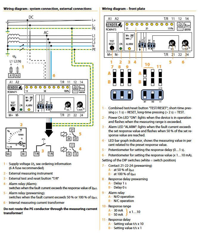
Adjustable response delay:
Alarm delay: 0… 10s infinitely adjustable, set through the potentiometer on the front panel, divided into two levels: x1 (0… 1s) and x10 (0… 10s), which can avoid false alarms (such as instantaneous current fluctuations during motor start-up) according to the on-site load characteristics.
Warning delay: 0s or 1s optional (DIP switch switching), quickly responding to potential risks while considering system stability.
Precision measurement mechanism:
Measurement core: Built in ø 18mm inner diameter measuring current transformer, using electromagnetic induction principle to monitor residual current, measurement results are almost unaffected by system load current and rated voltage, with strong stability.
Current type adaptation: It can accurately monitor 50Hz AC current, smooth DC current, positive and negative half wave pulsating DC current, phase controlled half wave current (delay angle 90 ° el/135 ° el), and half wave current with 6mA smooth DC superimposed, suitable for complex load scenarios.
(2) Operation and display functions
Multi functional operation button:
Built in combination “TEST/RESET” button: short press (<1s) for reset function, used to clear fault memory; Long press (>2s) is the testing function to verify whether the device monitoring and alarm circuit is working properly.
External Expansion: Supports connecting external test/reset buttons, with no hard limit on cable length, suitable for remote operation scenarios (such as operating outside the control cabinet).
Visual display system:
Power On LED: When the device is running normally, it stays on and flashes when the measured value exceeds the set range, providing quick feedback on the device’s working status.
Alarm LED: It stays on when the alarm threshold is reached and flashes when the warning threshold is reached, visually distinguishing between warning and alarm states.
LED bar chart indicator: displays the proportion of measured residual current to the set threshold at a scale of 0… 100%, with a total of 10 levels. It visualizes the trend of current changes in real time, making it easy for on-site personnel to quickly determine the level of risk.
Fault memory function: The alarm status is automatically stored inside the device and will not be lost even if the power is cut off. It needs to be cleared through a reset operation for easy fault tracing and cause analysis.
(3) Output and extension functions
Dual independent alarm relay:
Configure 2 conversion contacts (1 normally closed+1 normally open), support N/O (normally open) or N/C (normally closed) operation mode switching (DIP switch setting), can link warning and alarm circuits separately (such as warning trigger indicator light, alarm cut-off main power supply), adapt to different control logic requirements.
Relay parameters: rated contact voltage 150V AC/DC, rated current 5A, making capacity 2A (AC 230V, cos φ=0.4), breaking capacity 0.2A (DC 220V, L/R=0.04s), electrical life up to 12000 cycles, high reliability.
External device expansion:
Support connecting external measuring instruments, the device provides 0… 400 µ A current source output (corresponding to 0… 100% residual current ratio), load resistance ≤ 12.5k Ω, and can be connected to industrial grade display instruments for centralized monitoring.
Transparent sealing cover design: The front panel is equipped with a sealable transparent cover to prevent misoperation or malicious tampering of parameters, suitable for installation needs in industrial sites and public areas.
Detailed technical parameters
(1) Electrical parameters
Insulation and voltage resistance:
Rated insulation voltage: AC 250V, in compliance with IEC 60664-1 insulation coordination standard.
Rated impulse withstand voltage: 4kV, pollution level 3, with strong resistance to power grid surges and interference.
Power supply specifications:
Supply voltage (by model): RCMA475LY(230V AC/DC)、RCMA475LY-13(90…132V AC/DC)、RCMA475LY-21(9.6…84V AC/DC)、RCMA475LY-23(77…286V AC/DC), The 230V model is suitable for industrial and civilian scenarios, while the other models are designed specifically for industrial applications and can be customized with other power supply voltage versions as needed.
Working range of power supply voltage: 0.85… 1.1 x rated power supply voltage, suitable for voltage fluctuations in the power grid.
Power supply frequency range: DC/50… 60Hz, universal AC/DC power supply, suitable for different power supply environments.
Measurement accuracy and response characteristics:
Relative uncertainty of response value: ≤ 25%, small measurement error, high data reliability.
Lag characteristic: about 25% of the response value, avoiding frequent alarms caused by small fluctuations in current and improving system stability.
Response time: ≤ 70ms when the residual current is 1 times the alarm threshold (tv=0s); ≤ 40ms when the residual current is 5 times the alarm threshold (tv=0s), quickly respond to fault current and reduce safety risk exposure time.
(2) Environmental and mechanical parameters
Environmental adaptability:
Working environment temperature: -25…+70 ℃, can withstand severe cold and high temperature industrial environment.
Storage environment temperature: -40…+75 ℃, suitable for extreme temperature conditions of long-distance transportation and long-term storage.
Climate grade: DIN IEC 60721-3-3 (3K5), suitable for industrial scenarios with high dust and humidity.
Impact resistance: 15g/11ms during operation (IEC 60068-2-27), 40g/6ms during transportation (IEC 60068-2-29), vibration resistance: 1g/10… 150Hz during operation, 2g/10… 150Hz during transportation (IEC 60068-2-6), sturdy structure, strong resistance to harsh environments.
Mechanical structure:
Installation method: Supports screw installation (2 M4 screws, hole diameter 4.3mm) and DIN rail installation (compliant with IEC 60715 standard), can be embedded in standard distribution cabinets (compliant with DIN 43871 standard), and the installation position is not limited.
Shell specifications: Model X475, made of polycarbonate, with a flame retardant rating of UL94V-0, dimensions of 99mm × 91mm × 45mm (length × width × height), weight ≤ 350g, compact size, easy to install densely.
Protection level: The internal components and terminals have a protection level of IP30 (IEC 60529) to prevent solid foreign objects from entering.
(3) Wiring and connection parameters
Wiring terminals: Modular terminals are used, supporting rigid conductors (0.2… 4mm ²), flexible conductors (0.2… 2.5mm ²), and flexible conductors with/without plastic sleeves (0.25… 2.5mm ²), compatible with AWG 24… 12 specification conductors, with firm wiring and reliable contact.
Key wiring requirements:
The built-in measuring current transformer only passes through the phase line (L1, L2, etc.) and neutral line (N). PE conductors are strictly prohibited from passing through the transformer, otherwise it may cause measurement errors or equipment failure.
It is recommended to connect 6A fuses in series in the power supply circuit to protect the equipment from damage caused by power overcurrent.
External testing/reset buttons and external measuring instruments need to be connected to the corresponding terminals according to the wiring diagram to ensure stable signal transmission.
Working characteristics of different current types
RCMA475LY has strong adaptability to different types of fault currents, and the working current range (relative alarm threshold I Δ n) is as follows to ensure monitoring reliability in complex load scenarios:
Specific description of current type, working current range (relative to I Δ n), typical application scenarios
AC current 50Hz sine wave AC current 0.5… 1 × I Δ n for ordinary motors and lighting loads
Pulsating DC current positive and negative half wave pulsating DC (including half wave rectified current) 0.5… 1.4 × I Δ n single-phase rectified charger
Phase controlled half wave current delay angle of 90 ° el/135 ° el for phase controlled rectification current 0.5… 1.4 × I Δ n thyristor speed control equipment
Half wave current of mixed DC current combined with 6mA smooth DC, 0.5… 1.4 × I Δ n rectified load with filtering
Smooth DC current Pure DC fault current 0.5… 2 × I Δ n Battery powered equipment, DC-DC converter
Model specifications and ordering information
(1) Core model differentiation
Products are classified into models based on power supply voltage, and different models are suitable for different power supply scenarios. When ordering, it is necessary to clearly specify the model and order number:
Model, Supply Voltage Range, Applicable Scenarios, Order Number
RCMA475LY 230V AC/DC Industrial Application+Civil Building B 9404 2002
RCMA475LY-13 90… 132V AC/DC Industrial Application B 9404 2004
RCMA475LY-21 9.6… 84V AC/DC Industrial Application B 9404 2014
RCMA475LY-23 77… 286V AC/DC Industrial Application B 9404 2015
Note: Other power supply voltage versions can be customized according to users’ special needs. Please contact the manufacturer for confirmation.
(2) Recommended supporting components
To expand the functionality of the device, manufacturers provide dedicated supporting components that can be selected according to actual monitoring needs:
Component Name Function Description Model Order Number Key Parameters
External measuring instrument 0… 100% residual current ratio display 9604-4241 B 986 807 size 96 × 96mm, compatible with standard instrument panel installation
Measurement converter signal conversion (input → output) RK170 B 9804 1500 input 0… 400 µ A, output 0… 10V or 4… 20mA, compatible with PLC and DCS centralized monitoring systems
Installation and Operation Guide
(1) Installation points
Installation location: Choose an area with good ventilation, away from heat sources and strong electromagnetic interference sources, such as inside the distribution cabinet. The installation direction is not limited to ensure that the front panel is easy to operate and observe.
Wiring specifications: Strictly follow the wiring diagram to connect the power line, signal line, and load line. PE conductors must not pass through the built-in measuring current transformer. After wiring is completed, tighten the terminal screws to avoid loosening and poor contact.
Protective measures: The sealed transparent cover should be locked after the parameter settings are completed to prevent unauthorized personnel from tampering with the settings; Outdoor or dusty environments require additional protective covers to ensure a protection level of no less than IP30.
(2) Parameter setting steps
Threshold setting: Adjust the alarm threshold (30… 500mA) through the “x mA” potentiometer on the front panel. Rotate clockwise to increase and counterclockwise to decrease.
Mode switching: Set the warning ratio (50%/100% I Δ n1), warning delay (0s/1s), and relay mode (NO/NC) through DIP switches, with the white end of the switch indicating the effective position.
Delay setting: Adjust the alarm delay through the “t/s” potentiometer, switch the x1/x10 gear to select the delay range (0… 1s or 0… 10s).
Function test: Long press the “TEST/RESET” button (>2s) to start the test. The device should trigger the alarm relay action, and the LED bar graph should respond synchronously with the Alarm LED. After verifying that the device is functioning properly, short press to reset.
Product Name: FIO I/O Module with Built in Safety Barrier
Applicable environment: Installed in Zone 2 or Division 2 areas, it can connect to on-site devices located in Zone 0, 1, or Division 1 areas
Compliance standards: Compliant with ISA S71.04 class G3, meeting ATEX and FM certification requirements (subject to corresponding certificate “special conditions”)
Environmental adaptability: working/storage temperature * * -20~70 ℃**
Isolation characteristics: The on-site interface and system have galvanic isolation, while there is no isolation between channels
Key note: When multiple channels are short circuited, all channels of the module will lose their intrinsic safety function
Analog input module (isolated) ASI133 channels: 8 channels
Input signal: 4-20mA
Accuracy: ± 16 µ A
Input resistance (Power ON): 2-wire system 400-750 Ω, 4-wire system 485-925 Ω
Data update cycle: 10ms
Transmitter power supply: 16V DC or above (current limit 20mA), withstand voltage 1500V AC, maximum power consumption 5V 150mA/24V 450mA, weight ≈ 0.30kg, supports HART communication (- H model)
Analog output module (isolated) ASI533 channels: 8 channels
Output signal: 4-20mA
Accuracy: ± 48 µ A
Load resistance: 0-750 Ω at 20mA, 0-600 Ω at 23mA
Data update cycle: 10ms withstand voltage 1500V AC, maximum power consumption 5V 150mA/24V 350mA, weight ≈ 0.30kg, supports HART communication (- H model)
Input signal: RTD (Pt/Ni series 2/3/4 wires), POT (3-wire 0-10k Ω)
Accuracy: Pt100 ± 150m Ω, POT ± 2 Ω
Measurement current: 150 µ A, withstand voltage 1500V AC, maximum power consumption 5V 150mA/24V 60mA, weight ≈ 0.30kg, supports channel independent type selection
Digital input module (isolated) ASD143 channel count: 16 channels
Input signal: NAMUR (IEC 60947-5-6) compatible
Response time: Status input 15ms, button input minimum ON detection 20ms, withstand voltage 1500V AC, maximum power consumption 5V 150mA/24V 110mA, weight ≈ 0.30kg
Digital output module (isolated) ASD533 channel count: 8 channels
Output signal: 12V (40mA), 26V (0mA)
Response time: 10ms withstand voltage 1500V AC, maximum power consumption 5V 150mA/24V 500mA, weight ≈ 0.30kg
Intrinsic safety parameters (ATEX/FM)
(1) ATEX core parameters (some key modules)
Module model configuration method Uo (V) Io (mA) Po (mW) Co (nF) Lo (mH)
ASI133-S00/H00 single configuration (2-wire) 27.8 84 584 2 18
Data refresh cycle: 1 second per device (17 seconds per ESB bus connection for 16 devices)
Redundant configuration: Install 2 modules in adjacent slots (odd even slots), supporting dual redundant configuration
Model code and ordering
(1) Encoding rules (universal structure)
Encoding type meaning optional values
Main model module type identification ASI133 (analog input), ASI533 (analog output), AST143 (TC/mV input), etc
Suffix code 1 Function type – S (standard type), – H (with HART communication)
The suffix code 2/3 has a fixed code of 0
Option code terminal types/SA3S0 (analog input standard terminal),/SA3D0 (analog input redundant terminal), etc. (distinguished by module type)
(2) Ordering requirements
It is necessary to clearly specify the main model+suffix code+option code, for example: Analog input module with HART communication and standard terminals: ASI133-H00/SA3S0