Bender LifeGuard ® The LG2 series is an industrial grade ground fault protection panel launched by Bender, a German company. Its core function is to monitor the ground fault current in the circuit, quickly cut off the load power supply when the current reaches the trip threshold, and avoid safety risks such as electric shock and arc flashover. The product is compatible with various voltage and phase industrial circuits, providing flexible installation forms and operation methods, complying with UL 508A industrial control panel standards, and widely used in factory equipment, industrial control systems, and other scenarios.
Core parameters and specifications
Category specific parameters
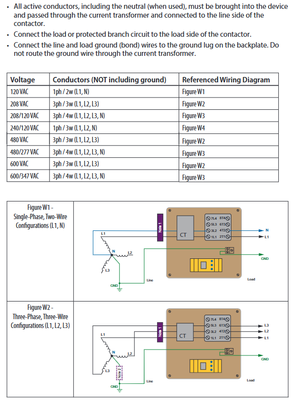
Adaptation voltage 120VAC、208VAC、208/120VAC、240/120VAC、480VAC、480/277VAC、600VAC、600/347VAC
Circuit phase 1ph (2w/3w), 3ph (3w/4w)
Rated current < 100A, 100A
Release level digital display fixed 6mA
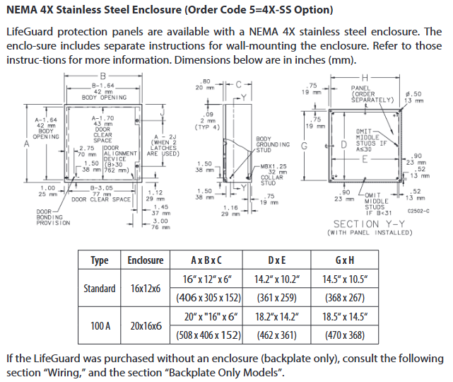
Shell type NEMA 4X polycarbonate, NEMA 4X stainless steel, backplate only (requires self provided cabinet)
ISOMETER ® The iso685 series is an integrated insulation monitoring and fault location device developed by Bender, a German company. It is designed specifically for IT systems (ungrounded systems), with the core mission of real-time monitoring of insulation resistance, DC offset voltage, and other parameters. Combined with EDS (Insulation Fault Locator), it achieves accurate fault location and avoids the risk of electric shock and equipment damage. The product is divided into D-type (integrated display/button) and S-type (no display, requiring FP200 panel). The W-enhanced type has higher anti vibration and anti temperature performance (-40~+70 ℃), suitable for complex scenarios such as industrial automation and ship power, and complies with international standards such as IEC 61557-8.
Core parameters and physical characteristics
Category specific parameters
Dimensions: Width 108mm, Height 93mm, Depth 110mm
Weight < 510g (excluding accessories)
Power supply requirements: AC/DC 24~240 V (tolerance -30%~+15%), frequency 50~400 Hz
Environmental adaptability standard type: working -25~+55 ℃, storage -40~+70 ℃; W-type: working -40~+70 ℃
Installation method: DIN rail installation (compliant with IEC 60715), screw installation (3 x M4 screws)
Adaptation system and measurement profile
(1) Scope of adaptation system
System type Voltage range Frequency range Maximum leakage capacitance
AC system 0~690 V (RMS) 0.1~460 Hz 0~1000 μ F (by profile)
DC system 0~1000 V -0~1000 μ F (according to profile)
3 (N) AC system 0~690 V (RMS) 50~60 Hz 0~150 μ F (power circuit profile)
(2) 6 measurement profiles
Profile type applicable scenario key parameters
Conventional constant frequency systems for power circuits measure a voltage of ± 50 V and a leakage capacitance of 0-150 μ F
Control circuits – Low voltage sensitive systems – Measurement voltage ± 10 V, voltage ≤ 230 V
Generator monitoring rapid measurement, frequency 50-60 Hz, leakage capacitance 0-5 μ F
Leakage capacitance of large capacitance systems such as ships with high capacitance ranging from 0 to 1000 μ F
Inverter>10 Hz (Inverter>10 Hz) 10~460 Hz Frequency conversion system leakage capacitance 0~20 μ F
Inverter<10 Hz (0.1~10 Hz) Low frequency system leakage capacitance 0~20 μ F
Detailed explanation of core functions
(1) Insulation monitoring function
Dual alarm setting: The response values of ALARM1 (warning) and ALARM2 (main alarm) can be independently set between 1 k Ω and 10 M Ω, with default values of 40 k Ω and 10 k Ω, respectively. It supports 25% hysteresis to prevent false alarms.
Connection monitoring: Real time detection of L1/+, L2, L3/- line connections and PE grounding status, triggering sound and light alarms in case of abnormalities.
Data storage: The historical memory can store 1023 alarm/fault information, including date and timestamp, and cache for 3 days after power failure.
IsoGraph trend chart: supports visualization of insulation resistance changes by hour/day/week/month/year, with up to 100 measurement points.
(2) Insulation fault location (EDS function)
Compatible with EDS devices: Supports EDS440-S/L (positioning current 2~10 mA), EDS441-S/L (positioning current 0.2~1 mA), and can connect up to 21 EDSs (255 channels).
Automatic mode: ALARM2 triggers and automatically starts, with a cyclic interruption for insulation measurement;
Cycle mode: ALARM2 triggers and starts one cycle before stopping.
Key parameters: The positioning current can be set to 1/1.8/2.5/5/10/25/50 mA, and the response value I Δ L (main alarm) is 200 μ A~10 mA.
(3) ISOnet system isolation
Function: Through Ethernet, multiple devices (≤ 20) can collaborate to ensure that only one device actively measures at a time, while the rest are isolated and in standby mode.
Configuration requirements: BCOM system name and subsystem address should be consistent, device address should be unique, and support automatic skipping of faulty devices.
Interface and Communication
Interface type communication protocol/functional key parameters
Ethernet (ETH) Modbus TCP, BCOM, Web Server 10/100 Mbit/s, up to 5 TCP connections
X1 multifunctional I/O digital input (3 channels), digital output (2 channels), analog output (1 channel), analog output supports 0~20 mA/0~10 V and other signals
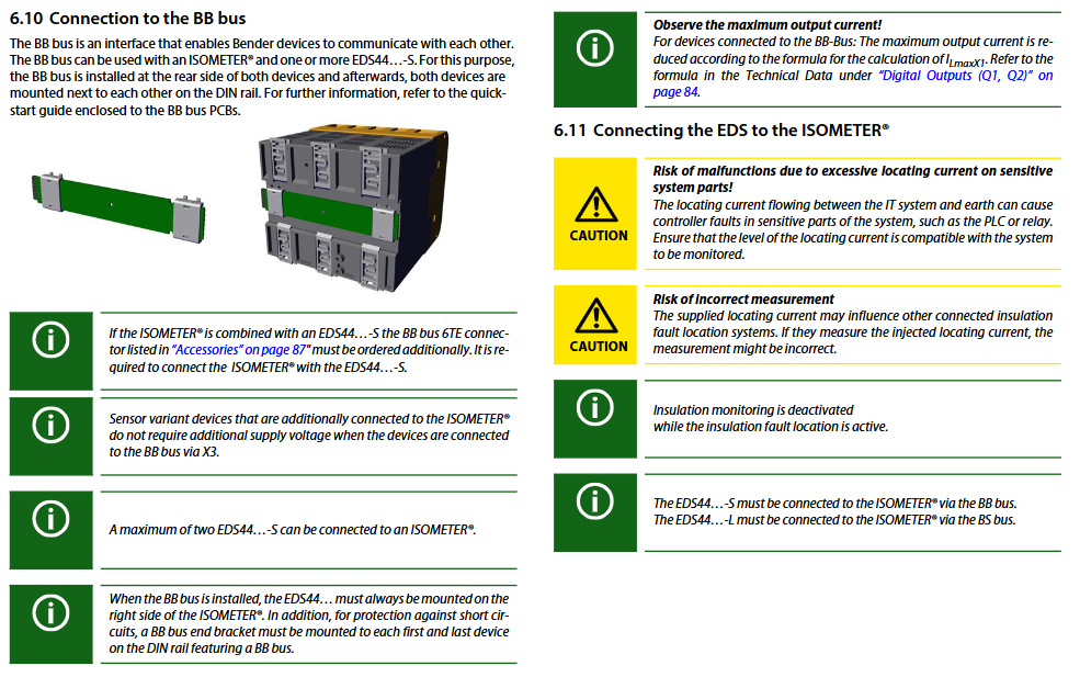
BB bus Bender internal device communication can connect up to 2 EDS44… – S devices without additional power supply
Web server remote parameter setting and data reading support Chrome/Firefox/Edge browsers, with write permission enabled
Operation and debugging process
(1) Basic debugging steps
Equipment installation: Choose the installation method, fix the equipment, and ensure the terminal spacing (horizontal 0mm, up and down 20mm);
Parameter configuration: Set language, date and time, system type, measurement profile, alarm response value, EDS mode, and positioning current through the debugging wizard;
EDS configuration: Scan EDS channel → Activate target channel → Set group parameters (CT type, response value, etc.);
Functional testing: Simulate insulation faults through grounding resistance to verify the accuracy of alarm triggering and fault location;
Operation monitoring: Check the standard display (insulation resistance+signal quality) and trace the data through isoGraph or historical memory.
(2) Alarm and fault handling
Alarm type triggering condition processing method
ALARM1 insulation resistance<Ran1 (default 40 k Ω) Observe the system status and troubleshoot if necessary
ALARM2 insulation resistance<Ran2 (default 10 k Ω), initiate EDS positioning, eliminate the fault, and reset
Check L1/+~L3/- wiring and PE connection for disconnection of faulty circuit or poor grounding of PE
EDS channel malfunction CT connection abnormality or channel not activated Rescan channel, check CT wiring
Maintenance and safety regulations
(1) Daily maintenance
No need for regular oil changes (sealed gearbox), if the cover is opened for maintenance, Mobil needs to be added ® 634 synthetic oil;
Regularly check the BS bus terminal resistance (120 Ω) to ensure stable communication;
Clean the display panel and terminals, ensure clear labeling and stickers, and replace worn parts in a timely manner.
(2) Safety regulations
Only professional personnel are allowed to install and debug. Before operation, the power must be turned off and the system must be confirmed to be out of power;
Power supply requires connection to a 24-240 V GFCI protection circuit, and modification of plugs/cables is prohibited;
When locating faults, avoid positioning current interference with sensitive components (such as PLC), and match the system tolerance value;
Only one device is allowed to actively measure in the coupled IT system, and the rest are isolated through ISOnet or digital input.
Ordering information and accessories
Product Model Description Product Number
Iso685-D-P with display/buttons, standard B91067030
Iso685W-D-P with display/buttons, W enhanced B91067030W
Iso685-S-P+FP200 without display+panel, standard type B91067230
The Greenlee 555C electric pipe bending machine is a professional bending tool launched by Greenlee, a subsidiary of Textron. It is designed for various types of conduits and pipes with specifications ranging from 1/2 “to 2”, and is mainly used in industrial electrical installation, building pipeline layout, and other scenarios. It can achieve precise and efficient bending operations. The product meets strict safety standards and is equipped with safety designs such as grounding protection and anti pinch point protection. It is paired with multiple sets of specialized bending accessories and detailed parameter tables to adapt to the bending needs of different pipes. The operation process is standardized to reduce operational difficulty.
IMC single boot set (01323) 1/2 “-2” IMC roller bracket assembly (78-3310-01323), to be paired with 02548 rigid/IMC curved boots
EMT single boot set (23803) 1/2 “-2” EMT curved boot (78-3310-02543), roller bracket (78-3310-02544)
PVC coated rigid single boot set (12586) 1/2 “-2” 40 mil PVC coated rigid conduit bending boot (78-3310-02553), roller bracket (78-3310-02554)
Operation process and bending type
(1) Basic operation steps
Equipment settings: Select the corresponding bending shoe and roller bracket, install and fix them, adjust the horizontal screw to level them;
Pipe marking: Mark the bending point on the pipe according to the bending type (such as 90 ° short pipe, offset bending) and parameter table;
Loading positioning: Place the pipe into the groove of the bent boot, align the mark with the front edge of the boot hook, and ensure that the pipe path is unobstructed;
Bending operation: Press the BEND key to start bending, release when approaching the target angle, and short press to fine tune to the precise angle;
Unloading reset: Press the UNLOAD button, rotate the bending shoe in the opposite direction, twist the pipe to detach from the hook, reset to 0 °, and prepare for the next operation.
(2) Main bending types and parameters
Bending type applicable scenario core parameter reference
90 ° short pipe vertical/horizontal pipeline turning minimum short pipe length=deduction value+2 inches, need to compensate for rebound angle
Deviation curve avoids obstacles with a deviation height of 2 “-22”, center distance=deviation height x angle coefficient (15 ° coefficient 3.9, 30 ° coefficient 2.0, etc.)
Three curved saddle crossing small obstacles requires marking three bending points, referring to the L1, L2, and Z parameter tables
Four curved saddle crossing large obstacles including straight sections design, requiring marking of four bending points
U-shaped reciprocating pipeline layout angle of 90 °, refer to the Y value and L1 parameter table
Safety operation standards
Electrical safety: Only connect 120V, 20A GFCI protection circuits, do not modify power cords and plugs, and replace damaged cables in a timely manner;
Environmental safety: Do not use in flammable or humid environments, avoid exposure to rain, and wear eye protection equipment during operation;
Mechanical safety: Keep hands away from pinch points such as bent boots and rollers, do not remove protective covers, and do not use equipment as ladders;
Operation safety: Before replacing accessories, the power must be cut off. When handling, ensure that the handle is securely installed (with safety spring clips and elastic pins fixed), and multiple people cooperate to handle heavy components.
Maintenance and troubleshooting
(1) Daily maintenance
The gearbox is designed for sealing and does not require regular oil changes; If the lid is opened for repair, it needs to be cleaned with kerosene and filled with 26 fluid ounces of Mobil ® 634 synthetic oil;
Regularly check the chain tension and maintain appropriate tension by adjusting the eccentric cam and reducer position, with a torque standard of 47 Newton meters (35 foot pounds);
Keep the equipment clean, ensure that the label stickers are clear and readable, and promptly replace worn or damaged bent boots, rollers, and other components.
(2) Common fault handling
Possible causes and solutions for the fault phenomenon
The device is unable to operate due to power supply failure and the switch is not turned on. Check the power supply circuit and confirm that the switch is in the ON position
Excessive bending angle of 1-1/2 “or 2” EMT/IMC compression is too tight. Rotate the adjusting bolt counterclockwise to reduce the compression force
Insufficient bending angle, loose compression, differences in pipe characteristics. Rotate the adjusting bolt clockwise to increase the compression force, or compensate for excessive bending appropriately
Motor overload tripping, mismatched pipe specifications, incorrect installation of rollers/boots. Confirm that the pipe is compatible with the accessories and reinstall the bent boots and rollers
Accessories and Parts Support
The product provides a complete accessory system, covering bending accessories, repair parts, tools and consumables, etc. The core accessories include:
ISOMETER ® Iso685 (W) – D/- S is a professional insulation monitoring equipment developed by Bender, a German company, specifically designed for IT systems (ungrounded AC/DC systems). Its core mission is to detect insulation faults in a timely manner by monitoring key parameters such as insulation resistance and DC offset voltage, avoiding risks such as electric shock and equipment damage. The product is divided into two variants: D-type (integrated graphic LC display and operation buttons) and S-type (no display/buttons, required to be used with FP200 (W) front-end panel), both supporting AC/DC/3 (N) AC system monitoring. With coupling equipment, the rated voltage monitoring range can be extended to 12 kV, meeting the needs of industrial scenarios with different voltage levels.
The product complies with international standards such as IEC 61557-8 and DIN EN 61557-8, and has high reliability and anti-interference ability. It is suitable for various scenarios such as industrial production lines, emergency power supply systems, and ship power, and is one of the core equipment to ensure the safe operation of the power system.
Core functions and features
(1) Monitoring and measurement functions
Insulation resistance monitoring
Measurement range: 0.1 k Ω~20 M Ω, alarm response value can be independently set within 1 k Ω~10 M Ω (ALARM1/ALARM2).
Preset response values: Factory default ALARM1=40 k Ω, ALARM2=10 k Ω, supports custom adjustment.
Measurement accuracy: ± 15% (minimum ± 1 k Ω), in accordance with the requirements of IEC 61557-8 standard.
Dual alarm mechanism: When the insulation resistance is lower than the corresponding response value, the relay action and LED indication are triggered, supporting fault memory (maintaining the alarm state until manual reset).
Multi parameter collaborative monitoring
DC offset voltage monitoring: A DC alarm threshold of 20 V~1 kV can be set to avoid the impact of DC components on the system.
System leakage capacitance monitoring: measurement range 0~1000 μ F, accuracy ± 10% (minimum ± 10 μ F), equipment automatically adapts to capacitance changes.
Connection monitoring: Real time monitoring of the connection status of the measurement line to avoid monitoring failure caused by line disconnection.
The multi measurement profile adaptation device provides 7 measurement profiles, which can be flexibly selected according to the system type to optimize measurement speed and accuracy:
Profile type applicable scenario key parameters
Power circuits – Conventional constant frequency systems with voltages ranging from 0 to 690 V (AC)/0 to 1000 V (DC) and capacitors ranging from 0 to 150 μ F
Control circuits: Low voltage sensitive control system measures voltage ± 10 V, voltage 0-230 V (AC/DC)
Generator monitoring rapid measurement, frequency 50-60 Hz, capacitance 0-5 μ F
High capacitance systems such as ships have a capacitance of 0~1000 μ F and a voltage of 0~690 V (AC)/0~1000 V (DC)
Variable frequency converter>10 Hz (inverter>10 Hz) 10~460 Hz Variable frequency system capacitance 0~20 μ F, voltage 0~690 V (AC)/0~1000 V (DC)
Frequency converter<10 Hz (inverter<10 Hz) 0.1~10 Hz Low frequency system capacitance 0~20 μ F, voltage 0~690 V (AC)/0~1000 V (DC)
Customer specific special needs scenarios are defaulted to be consistent with the power circuit profile and support Bender customization
(2) Display and storage functions
Graphic display: equipped with a 127 × 127 pixel graphic LC display screen, real-time display of insulation resistance, alarm status, signal quality and other information, supporting multilingual switching (including English, German, etc.).
Historical memory: It can store 1023 alarm/fault information, each record containing date, time, fault type, and measurement value, and data will not be lost after power failure (continuous fault memory mode).
Trend analysis: The isoGraph function can graphically display the insulation resistance change trends for 1 hour, 1 day, 1 week, 1 month, and 1 year, facilitating fault tracing and system status prediction.
(3) Communication and Control Interface
The device supports multiple communication methods to achieve local and remote control:
Interface type communication protocol/functional key parameters
Ethernet (ETH) Modbus TCP, BCOM, Web Server 10/100 Mbit/s, supports DHCP/static IP, up to 5 TCP connections
X1 multifunctional I/O digital input (3 channels), digital output (2 channels), analog output (1 channel), analog output supports signals such as 0~20 mA/4~20 mA/0~10 V, etc
Relay output 2 conversion contacts (K1/K2) support N/C/N/O mode, AC-13 class 230 V/5 A, electrical life 10000 times
(4) Safety and operational assurance
Safety protection: Terminal protection level IP20 (external)/IP30 (internal components), shell flame retardant level UL94 V-0, with overvoltage and overcurrent protection.
Operation protection: Supports 4-digit password protection (0000~9999) to prevent unauthorized parameter modification; Continuous self-test function, automatically detects internal circuits, measurement circuits, and connection status after startup.
Convenient operation: Parameter setting, alarm reset, and self detection can be achieved through buttons such as MENU/TEST/RESET, and support remote parameter modification on web servers (with write permission enabled).
Model specifications and ordering information
(1) Core model parameters
Model Equipment Type Power Supply Voltage Protection Enhancement (Option W) Product Number
Iso685-D with display/button AC/DC 24~240 V No B91067010
Iso685W-D with display/button AC/DC 24~240 V (-40~+70 ℃, anti vibration) B91067010W
Iso685-S+FP200 no display+panel AC/DC 24~240 V No B91067210
Iso685W-S+FP200W without display+panel AC/DC 24~240 V is B91067210W
After the device is connected to the power supply, it automatically starts self detection (15-20 seconds) to detect the internal circuit, measurement circuit, and grounding connection.
After passing the self-test, enter the normal monitoring mode and continuously collect parameters such as system insulation resistance and leakage capacitance.
When the insulation resistance is lower than the set response value, the response delay is activated (can be set to 0-300 seconds), and the corresponding alarm relay and LED indicator are triggered after the delay is over.
After troubleshooting, the parameters are restored to the release value (response value+25% hysteresis), the release delay is initiated, and the relay is reset after completion; When the fault memory is activated, the RESET button needs to be manually pressed to reset.
(2) Debugging process
Initial debugging: Connect the device → Connect the power supply → Run the debugging wizard (set language, date and time, system type, measurement profile, alarm response value) → Perform functional testing (simulate faults through grounding resistance).
Password configuration: Set a 4-digit password in the device menu, and verify it before modifying parameters.
Remote configuration: remotely read measurement values and modify parameters (with write permission enabled) through a web server (input device IP) or Modbus RTU protocol.
Typical application scenarios
Industrial power system: Monitor the insulation status of generators, frequency converters, and transformers to prevent equipment failures caused by insulation degradation.
Emergency power supply system: Insulation monitoring of backup power sources such as UPS and diesel generators to ensure the safety of power supply in emergency situations.
High capacitance scenario: For large leakage capacitance systems such as ships and rail transit, monitoring accuracy is optimized through “high capacitance” measurement profiles.
Low voltage control system: Insulation protection for industrial automation control circuits to prevent damage to sensitive components due to insulation faults.
Medium and high voltage expansion: Equipped with AGH series coupling equipment, monitor the insulation status of medium and high voltage IT systems such as 6 kV and 12 kV.
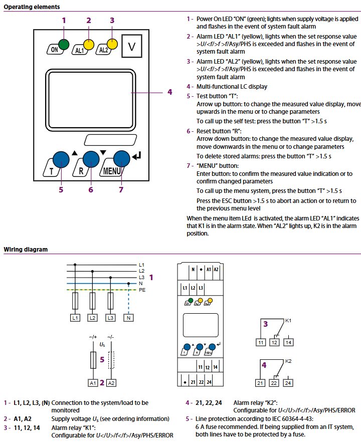
LINETRAXX ® VMD420 is a multifunctional voltage frequency monitor launched by BENDER, designed specifically for 3 (N) AC systems. Its core is used to monitor voltage (under voltage, over voltage), frequency (under frequency, over frequency), and phase related parameters (phase sequence, phase loss, asymmetry). The measurement voltage range covers 0… 500 V (L-L)/0… 288 V (L-N), and the frequency range is 15… 460 Hz. It adopts true RMS (AC+DC) measurement method to ensure data accuracy. The product complies with CE, DIN EN 45545-2, and IEC series standards, with high reliability and industrial grade protection performance, suitable for various electrical safety monitoring scenarios.
Core functions and features
Functional category, specific content, key parameters/description
Monitoring function: Voltage monitoring for undervoltage (U<) and overvoltage (U>), with a resolution of 1 V and a preset value of 0.85Un (undervoltage)/1.1Un (overvoltage)
Frequency monitoring under frequency (<f), over frequency (>f), set resolution to 0.1 Hz (10.0… 99.9 Hz)/1 Hz (100… 500 Hz)
Response speed, voltage action time ≤ 140 ms, frequency action time ≤ 335 ms
Display and Storage: Multi functional LC non luminous display screen, real-time display of measured values (0… 500 V)
Storage function operation value memory, first alarm value history record, fault memory (supports on/off/con mode, optional power-off hold)
Security and operational protection features include password protection (0… 999), sealed transparent cover, continuous self-monitoring, and test/reset button
Output configuration includes 2 independent alarm relays (K1/K2), supporting N/C/N/O switching and configurable monitoring types
Technical parameter details
1. Power supply and model information
Model Supply Voltage (Us) Frequency Range Terminal Type Product Number (Art. No.)
VMD420-D-1 AC 16… 72 V/DC 9.6… 94 V 15… 460 Hz screw terminal B93010005
Insulation performance: rated insulation voltage of 400 V, rated impulse voltage of 4 kV (pollution level III), maximum withstand voltage test of 3.32 kV
Measurement accuracy: Voltage ± 1.5% (50/60 Hz), ± 3% (15… 460 Hz); Frequency ± 0.2% (15… 460 Hz)
Relay parameters: Contact type is conversion contact, 230 V/5 A under AC-13 category, 24 V/1 A under DC-12 category, electrical life of 10000 cycles
Power consumption: ≤ 4 VA
3. Environment and installation parameters
Category specific parameters
Temperature range: -25…+55 ℃; Transportation/Storage: -25…+70 ℃
Installation method: rail installation (compliant with IEC 60715) or screw installation (accessory B98060008 required)
Two module design for shell size, 36 mm (width) x 93 mm (height) x 90 mm (depth)
Wiring specifications for screw terminals: rigid 0.2… 4 mm ², flexible 0.2… 2.5 mm ²; Push in terminal: rigid 0.2… 2.5 mm ²
Typical application scenarios
Voltage sensitive equipment monitoring: protecting precision instruments, industrial controllers, etc. from voltage/frequency fluctuations;
Mechanical equipment control: automatically start and stop machinery and equipment according to the set voltage threshold;
Backup/Emergency Power Monitoring: Monitor the voltage and frequency stability of backup power supply systems such as UPS and generators;
Three phase motor protection: prevent motor damage caused by phase loss, open circuit, and asymmetric load;
Transformer protection: Identify asymmetric loads to avoid transformer overload or failure.
Operation and Configuration
Preset function (PrE run): automatically detects the rated system voltage after the first connection, sets the undervoltage/overvoltage/underfrequency/overclocking response values, and displays “AL not SET” when no voltage is detected, which needs to be manually configured;
Key operation: Parameter setting, alarm reset, and self-test functions can be achieved by testing (T), resetting (R), and menu (MENU) keys. Long pressing (>1.5 s) can call advanced functions;
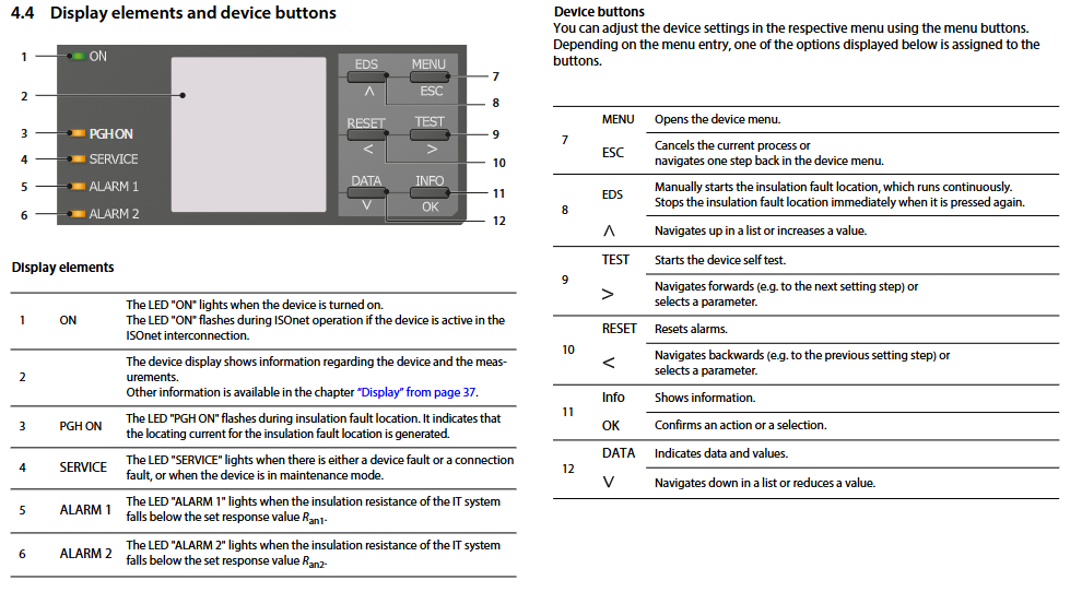
Meaning of indicator lights: When the power light (green ON) is on, it indicates that the power supply is normal, and when the alarm light (yellow AL1/AL2) is on/flashing, it indicates that the corresponding relay has triggered an alarm.
Key issues
Question 1: LINETRAXX ® What is the core monitoring range and accuracy of VMD420, and which power supply systems is it applicable to?
Answer: The core monitoring range includes voltage (L-L: 0… 500 V, L-N: 0… 288 V), frequency (15… 460 Hz, display range 10… 500 Hz), as well as phase sequence, phase loss, and asymmetry (5… 30% adjustable); The measurement accuracy is ± 1.5% (50/60 Hz)/± 3% (15… 460 Hz) for voltage and ± 0.2% (15… 460 Hz) for frequency. Suitable for 3 (N) AC systems, supporting two power supply versions: VMD420-D-1 (AC 16… 72 V/DC 9.6… 94 V) and VMD420-D-2 (AC/DC 70… 300 V), covering industrial low-voltage power supply scenarios.
Question 2: What are the flexible configuration options for alarm output and delay settings of this device?
Answer: Alarm output configuration: Equipped with 2 independent conversion contact relays (K1/K2), which can be configured to monitor 8 types such as undervoltage, overvoltage, frequency abnormality, phase sequence error, etc. It supports N/C (normally closed) or N/O (normally open) mode switching, and the fault memory can be set as “keep alarm”, “automatic reset” or “power-off hold”. Delay setting options: Start delay (0… 300 s to avoid false alarms during the startup phase), response delay (ton1/2:0… 300 s to filter short-term fluctuations), release delay (toff: 0… 300 s to ensure system stability and reset), delay setting resolution is 0.1 s/1 s/10 s depending on the interval (0… 10 s/10… 99 s/100… 300 s), suitable for different industrial scenarios.
Question 3: LINETRAXX ® What are the key precautions for the installation and operation of VMD420?
Answer: Installation precautions: ① The installation method supports rail (IEC 60715) or screw installation (requires accessory B98060008), with a housing size of 36 mm and sufficient heat dissipation space reserved; ② When wiring, attention should be paid to the wire specifications corresponding to the terminal type (screw/push in type), with a stripping length of 8-9 mm (screw terminal)/10 mm (push in type terminal) and a tightening torque of 0.5… 0.6 Nm; ③ Line protection should be equipped with 6A fuses according to IEC 60364-4-43 standard, and dual line fuse protection is required for IT system power supply. Precautions for operation: ① It is recommended to enable the preset function (PrE run) to automatically configure basic parameters when using for the first time. If no voltage is detected, the response value needs to be manually set; ② Password protection is turned off by default, and 0… 999 passwords can be set to prevent accidental operations; ③ Alarm reset requires long pressing the reset button (R>1.5 s). When the fault memory is in “con” mode and the power is turned off, the alarm parameters remain unchanged.
The Current Tools 77 series electric pipe bending machine is a professional equipment designed specifically for industrial pipeline installation. It features “single shoe adaptation to multiple specifications, sturdy structure, and easy maintenance”, and can meet the bending needs of different types of pipelines (EMT, IMC, Rigid, PVC coated Rigid) ranging from 1/2 “to 2”. It is widely used in construction, electrical installation, and other scenarios. The product is manufactured in the United States, with strict quality control and a two-year warranty. The core electrical components are the same as the 747 Omni of the same brand ™ The pipe bending machine is interchangeable, reducing maintenance costs.
Product model and core configuration
(1) Host model classification
Host model, compatible with pipeline type, including component weight, UPC code
77 without (power unit only) electric power source (without boots and roller bracket) 270 lbs 811993020261
77SR 1/2 “-2” Rigid Pipe Power Unit+Rigid Single Shoe+Rigid Roller Bracket 334 lbs 811993025495
77SI 1/2 “-2” IMC pipeline power unit+IMC single boot+IMC roller bracket 369 lbs 811993025501
77SE 1/2 “-2” EMT pipeline power unit+EMT single boot+EMT roller bracket 361 lbs 811993025518
77SP 1/2 “-2” PVC coated Rigid pipe power unit+PVC coated Rigid single boot+corresponding roller bracket 330 lbs 811993025525
(2) Single boot model and components
All single boot sets include “single boot+roller bracket+metal storage box” and are compatible with Greenlee ® five hundred and fifty-five ® The classic pipe bending machine has the following specific configuration:
Shoe set model, compatible with pipeline type, component details (including model), weight of each component, total UPC code
700SR 1/2 “-2” Rigid 1. Single boot (2-3000); 2. Roller bracket (2-4000); 3. Metal storage box (8-0501) single boot 51 lbs; Roller bracket 13 lbs; Storage box 36 lbs 811993025419
700SI 1/2 “-2” IMC 1. Single boot (2-3000); 2. Roller bracket (2-4100); 3. Metal storage box (8-0501) single boot 51 lbs; Roller bracket 48 lbs; Storage box 36 lbs 811993025426
700SE 1/2 “-2” EMT 1. Single boot (2-3100); 2. Roller bracket (2-4200); 3. Metal storage box (8-0501) single boot 43 lbs; Roller bracket 48 lbs; Storage box 36 lbs 811993025433
700SP 1/2 “-2” PVC coated Rigid 1. Single boot (2-3200); 2. Roller bracket (2-4300); 3. Metal storage box (8-0501) with a single boot weighing 47 lbs; Roller bracket 13 lbs; Storage box 36 lbs 811993025440
Special note: When bending 1 1/2 “and 2” Rigid aluminum pipes, an IMC single shoe roller bracket (model 2-4100) is required.
Core technical parameters
(1) Basic parameters
Parameter category specific specifications
Power requirement: 120V AC, 20A GFCI protective socket (220V version requires consultation with the factory)
No PC board design: using simple and reliable electrical components to reduce the probability of electronic failures and improve equipment stability.
Detachable handle: supports doggle bends, suitable for pipeline forming requirements in complex installation scenarios.
Non inflatable wheels: convenient for equipment movement and reduce on-site maintenance frequency.
Compatibility and maintainability:
Shoe set compatibility: All single boots and roller mounts can be adapted to Greenlee ® five hundred and fifty-five ® Classic pipe bending machine enhances the versatility of accessories.
Component exchange: Main electrical components and Model # 747 Omni ™ The pipe bending machine is interchangeable, reducing the cost of spare parts procurement.
Easy to maintain: With a simple structure and convenient troubleshooting, basic maintenance can be completed without the need for professional skills.
Manufacturing and Quality:
Made in the United States: Following strict industrial production standards to ensure equipment durability and service life.
Two year warranty: covering the core components of the host, providing users with long-term use guarantee.
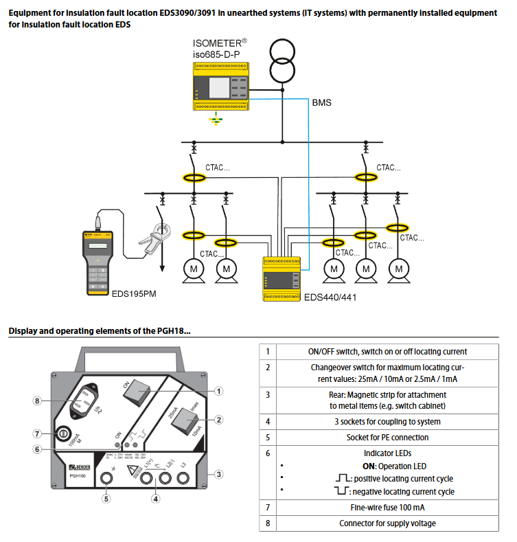
Brand and positioning: The EDS3090 series, launched by the German company BENDER, is a portable electrical detection device that integrates “ground fault location” and “residual current measurement”. Its core positioning is as a safety monitoring tool for ungrounded (floating) AC/DC systems, with a focus on “wide voltage coverage, dual function measurement, and portable and easy operation”. It can accurately locate faults to the load level in the online live state of the system, and also supports residual current measurement of branches of grounded/high resistance grounded AC systems. It is suitable for multiple scenarios such as industrial main distribution networks, ships, medical places, and small control systems.
Core design highlight: All components are stored in a sturdy aluminum chassis (size 430 × 340 × 155mm) with a weight of ≤ 9kg, making it easy to carry on site; Certified according to standards such as IEC 61326-2-4, it has industrial grade characteristics such as resistance to electromagnetic interference and wide temperature operation, meeting the requirements for use in harsh environments.
Product series classification and core differences
This series is divided into three dimensions based on “adaptation scenario, working mode, and power supply voltage”, with each model accurately matching different needs. The core differences are as follows:
Model Series Adaptation Scenarios Operating Modes Power Supply Voltage Core Components (Standard) Rated Voltage Range (Basic Configuration)
EDS3090 main distribution system is equipped with BENDER fault detectors – EDS195P, PSA3020 (20mm clamp), PSA3052 (52mm clamp) AC 20-575V (42-460Hz), DC 20-504V
EDS3090PG main distribution system independent (including current injector) 230V AC EDS195P, PGH185, PSA3020, PSA3052 are the same as EDS3090 (AGE185 extended to AC 500-790V, DC 400-960V)
EDS3090PG-13 Main Distribution System Independent (including current injector) 90-132V AC EDS195P, PGH185-13, PSA3020, PSA3052 Same as EDS3090
EDS3096PG offline system independent (including current injector) 230V AC EDS195P、PGH186、PSA3020、PSA3052 AC 0-575V(42-460Hz)、DC 0-504V
EDS3096PG-13 offline system independent (including current injector) 90-132V AC EDS195P, PGH186-13, PSA3020, PSA3052 are the same as EDS3096PG
EDS3091 small system/medical facility with installed BENDER fault detector – EDS195P, PSA3320 (20mm clamp), PSA3352 (52mm clamp) AC 20-265V (42-460Hz), DC 20-308V
EDS3091PG Small System/Medical Facility Independent (including Current Injector) 230V AC EDS195P, PGH183, PSA3320, PSA3352 Same as EDS3091
EDS3091PG-13 Small System/Medical Facility Independent (Including Current Injector) 90-132V AC EDS195P, PGH183-13, PSA3320, PSA3352 Same as EDS3091
I Δ s mode: Grounding fault location in ungrounded systems, receiving positioning current signals collected by measuring pliers;
I Δ n mode: residual current measurement of the grounding system, displaying the residual current value of the branch.
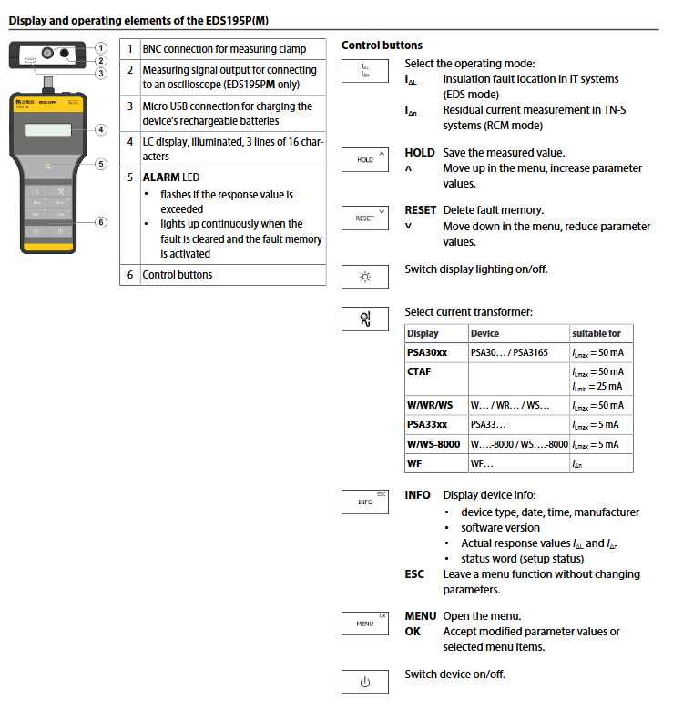
Key features: 3-line 16 character backlit LCD display screen, ALARM LED alarm light (lights up when the threshold is exceeded); Support HOLD data retention, RESET reset, and INFO device information query; Charging through MicroUSB interface.
Power supply and endurance: 3 AA batteries or NiMH rechargeable batteries (≥ 2000mAh), endurance ≤ 60h without backlight, power consumption ≤ 0.5W.
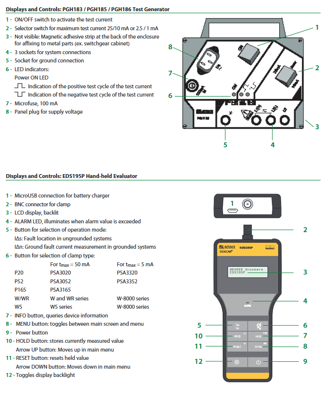
The PGH series current injector (positioning signal source) is responsible for generating stable positioning current and driving the fault location of ungrounded systems. Different models have clear adaptation scenarios: | Model | Adaptation Scenario | Power Supply Voltage | Maximum Positioning Current (optional) | Core Features|
|PGH183 | Small systems/medical facilities | 230V AC/90-132V AC (-13) | 1mA/2.5mA | Low current output, compatible with control circuits|
|PGH185 | Main distribution system | 230V AC/90-132V AC (-13) | 10mA/25mA | Medium high current output, compatible with main circuit|
|PGH186 | Offline System | 230V AC/90-132V AC (-13) | 10mA/25mA | Built in 50V DC Measurement Voltage, Suitable for Offline/Low Voltage Systems|
Operation design: including ON/OFF switch, current gear switch, back with magnetic strip (attached to metal cabinet), equipped with power ON and positive and negative current cycle LED indicator lights.
AGE185 voltage coupler (optional)
Function: Expand the system voltage range to AC 500-790V (42-460Hz), DC 400-960V, and adapt to high-voltage ungrounded systems;
Common features: All are equipped with 2m long shielded wires, connected to EDS195P through BNC connectors, and comply with CAT III (AC 600V)/CAT IV (AC 300V) safety levels.
Key technical parameters
(1) Measure performance parameters
Measurement Function Adaptation System Core Parameters Measurement Accuracy Frequency Range
Grounding fault location (main circuit) Non grounded AC/DC system response value: 2-10mA (default 5mA), positioning current: 10-25mA ± 30%/± 2mA AC 42-460Hz
Grounding fault location (control circuit) Non grounded AC/DC system response value: 0.2-1mA (default 0.5mA), positioning current: 1-2.5mA ± 30%/± 0.2mA AC 42-460Hz
Residual current measurement (30 series clamp) grounding/high resistance grounding AC system measurement range: 2mA-10A, response value: 10mA-10A (default 100mA) 42-60Hz: ± 5%; 61-1000Hz:±20% AC 42-1000Hz
Residual current measurement (33 series clamp) grounding/high resistance grounding AC system measurement range: 0.2mA-2A, response value: 5mA-1A (default 100mA) with the same accuracy as above AC 42-1000Hz
(2) Environmental and physical parameters
Parameter category specific specifications
Working temperature -10 ℃~+55 ℃
Climate level (IEC 60721): Fixed use 3K5, transportation 2K3, long-term storage 1K4 (no condensation, no icing)
The basic configuration of the chassis weight is ≤ 7kg, including PSA3165 pliers ≤ 8.5kg, EDS3092 model ≤ 9kg
Operation and usage characteristics
Core operating procedures
Mode switching: Use the EDS195P mode selection key to switch between “Fault location (I Δ s)” or “Residual current measurement (I Δ n)”;
Clamp type selection: Match the corresponding type (such as P20=PSA3020/3320) with the selection key based on the measurement clamp model used;
Data processing: Press the HOLD button to save the current measurement value, and press the RESET button to reset; The MENU key enters the parameter adjustment interface (such as response value, harmonic setting);
Alarm indication: When the measured value exceeds the set threshold, the ALARM LED lights up to indicate a fault.
Typical application scenarios
Scenario 1: Independent online fault location (without installed equipment): EDS3090PG/3091PG series, generates positioning current through PGH injector, and EDS195P cooperates with measuring pliers to locate the fault branch;
Scenario 2: In conjunction with the installed equipment fault location: EDS3090/3091 series, using existing detectors such as BENDER IRDH575 to generate signals, only the evaluation instrument and measuring pliers are needed to complete the positioning;
Scenario 3: Measurement of residual current in grounding system: All models support it. Wrap the branch cable with measuring pliers and directly read the residual current value.
Ordering and Accessories
Optional accessories and functions | Accessory name | Function description | Adaptation scenario|
|PSA3165 measuring pliers | 115mm large clamp, suitable for thick cables | measurement of large section cables in the main distribution system|
|AGE185 voltage coupler | extends voltage range to AC 500-790V/DC 400-960V | high voltage ungrounded system|
|EDS145-SET | Special accessories for fault location of diode isolation system | Power plant diode isolation DC system|
Example of ordering code:
EDS3090PG-13: Main distribution system, independent, 90-132V AC power supply, including PGH185-13 injector;
EDS3091PG: Small system/medical facility, standalone, 230V AC power supply, including PGH183 injector.
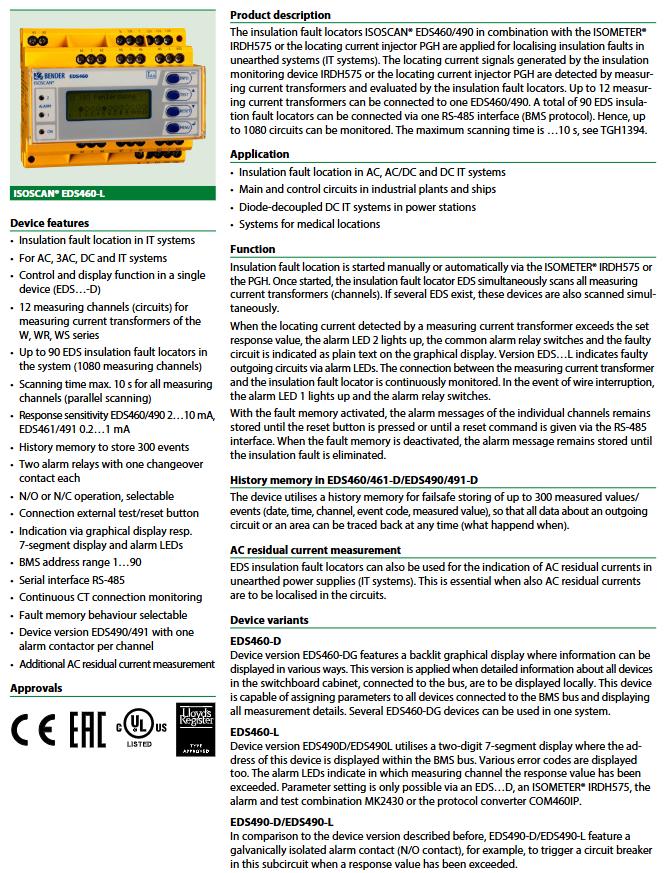
Brand and positioning: ISOSCAN launched by German company BENDER ® The EDS460/490-EDS461/491 series is an industrial grade equipment that integrates “insulation fault location” and “AC residual current measurement (RCM)”. Its core positioning is as an electrical safety monitoring tool for IT systems (ungrounded low-voltage distribution systems). It features “multi-channel, networking, and high sensitivity” and is suitable for AC, DC, and AC/DC hybrid IT systems. It is widely used in industrial plants, ships, power station diode isolated DC systems, and medical places.
Core design objective: Through collaboration with ISOMETER ® The IRDH575 insulation monitoring instrument or PGH positioning current injector is used in conjunction to quickly locate insulation fault points in the IT system, while monitoring residual current to ensure stable system operation and reduce electrical safety risks.
Product series classification and core differences
This series is divided into three dimensions based on “response sensitivity, display type, and alarm contact configuration”, with each model accurately adapting to different scenarios. The core differences are as follows:
Series classification dimensions, specific types, core features, and adaptation scenarios
Response sensitivity EDS460/490 insulation fault location response value 2… 10mA; residual current measurement 100mA… 10A main circuit, industrial general scenario
EDS461/491 insulation fault location response value 0.2… 1mA; residual current measurement 10mA… 1A control circuit, medical field (high sensitivity requirement)
Display type D (EDS46x-D/EDS49x-D) backlit graphic LCD display screen, supporting parameter settings, event queries, and multiple languages (German/English/French) that require local viewing of detailed data and on-site parameter configuration scenarios
L-type (EDS46x-L/EDS49x-L) 2-digit 7-segment digital tube+LED indicator light, only displays device address/error code, needs to be configured through D-type equipment or upper computer without on-site operation, only requires fault alarm indication scenario
Alarm contact configuration 46x series (EDS460/461-D/L) 2 common alarm relays (1 conversion contact per group) only require overall fault alarm, without the need for channel control scenarios
The 49x series (EDS490/491-D/L) includes 2 public alarm relays and 12 independent alarm relays (each with 1 normally open contact) that need to trigger protection actions (such as circuit breaker tripping) in different channels
| Insulation fault location response value | 2… 10mA | 0.2… 1mA | AC residual current measurement range | 100mA… 10A | 10mA… 1A | | Number of channels (single device) | 12 (supporting W/WR/WS series measurement current transformers) | 12 (supporting dedicated high-sensitivity measurement current transformers) | | | Maximum number of networking devices | 90 (total 1080 measurement channels) | 90 (total 1080 measurement channels) | | Full channel scanning time | Approximately 8… 24 seconds | Approximately 14… 30 seconds | | Response delay (t_on)) | 0… 24s (adjustable) | 0… 24s (adjustable) | | Release delay (t_off) | 0… 24s (adjustable) | 0… 24s (adjustable)|
Environmental and Physical Parameters | Parameter Categories | Specific Specifications |
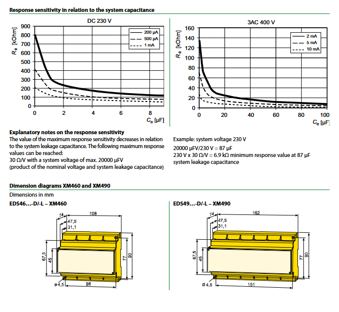
| Operating Temperature | -25…+55 ℃ | | Climate Class (IEC 60721) | Fixed Use 3K5, Transport 2K3, Long Term Storage 1K4 (No Condensation, No Ice) | | Mechanical Class (IEC 60721) | Fixed Use 3M4, Transport 2M2, Long Term Storage 1M3 | Protection Class (Terminal) | IP20 (DIN EN 60529) | | Shell Material | Polycarbonate (UL94 V-0 Flame Retardant Class) | | Weight | EDS46x Series ≤ 360g | | Installation Method | Screw Installation (2 × M4) or DIN Rail Installation (Compliant with IEC 60715) The sentence is:|
Interface and networking parameters | Interface type | Specific specifications |
| Communication interface | RS-485, supporting BMS protocol | | Baud rate | 9.6kbit/s | | Maximum cable length | 1200m (exceeding DI-1DL repeater required) | | Recommended cable | Twisted pair J-Y (St) Y, minimum 2 × 0.8mm ², shielding layer connected to PE | | Terminal resistance | 120 Ω (0.25W), enabled through DIP switch | Device address range | 1… 90 (BMS bus address)|
Core functions and operational features
Measurement and positioning function
Insulation fault location: By measuring the current transformer to collect the positioning current generated by the PGH injector or IRDH575, when the current exceeds the set response value, the ALARM 2 indicator light is triggered to light up, the D-type equipment displays the fault channel plaintext, and the corresponding channel LED of the L-type equipment lights up.
Residual current measurement: Monitor the AC residual current in the IT system, and when it exceeds 10A (EDS460/490) or 1A (EDS461/491), trigger the ALARM 1 indicator light to turn on.
Channel connection monitoring: Continuously monitor and measure the connection status between the current transformer and the equipment, and trigger the ALARM 1 indicator light to light up when there is a disconnection or short circuit (this function can be disabled).
Storage and alarm function
Historical storage: The D-type device has a built-in historical memory that can store 300 event records, including date, time, channel, event code, measurement value, and supports traceability queries.
Fault memory: “Fault memory activation” (alarm information retained until manual reset or bus reset) or “Fault memory deactivation” (alarm information retained until fault elimination) can be selected.
Alarm relay: supports normally open (N/O) or normally closed (N/C) operation mode selection, and the common alarm relay can be linked to external alarm devices or control systems.
Operation and configuration features
Operation buttons: D-type devices include buttons such as INFO (information query), TEST (self-test), RESET (reset), MENU (menu), etc; L-shaped devices only include basic settings and reset buttons.
Parameter configuration: D-type devices can locally set bus addresses, response delays, fault memory modes, etc; L-type equipment needs to be configured through D-type equipment, IRDH575, MK2430 alarm test combination, or COM460IP protocol converter.
External control: Supports connecting external test/reset buttons (cable length 0… 10m), external buttons of multiple devices cannot be connected to each other.
Core components and accessories
Supporting measurement current transformer: BENDER dedicated measurement current transformer is required, and different models are compatible with different equipment series. The core models are as follows: | Equipment series | Recommended transformer types | Transformer structure | Inner diameter specification (mm) | Model example | Accessory code | | ————–; Rectangle: 70×175, etc; Opening and closing type: 20×30/50×80, etc. | W20 (circular 20mm) | B98080003 | | EDS461/491 | W/WS-8000 series | Circular/opening and closing type | Circular: 20/35/60; Opening and closing: 20×30/50×80 | W20-8000 (round 20mm) | B98080009|
Auxiliary Accessories | Accessory Type | Function Description | Model | Accessory Code |
| RS-485 Repeaters | Extended Bus Distance (over 1200m) or Number of Extended Devices (over 32 units) | DI-1DL | B95012047 | | USB Powered, No Additional Power Supply | DI-2USB | B95012045 | Protocol Converter | BMS Bus to TCP/IP (Ethernet) | COM460IP | B95061010 | | | BMS Bus to Modbus/RTU | FTC470XMB | B95061002 | | BMS Bus to PROFIBUS DP | FTC470XDP | B95061000 | | Power Adapter | Power Supply for Repeaters DI-1/DI-2 | AN471 B924189|
Power supply specifications and ordering information
Power supply voltage options: The device provides two power supply specifications, suitable for different industrial scenarios: | Power supply type | Specification parameters | Corresponding model suffix |
Typical ordering code example:
EDS460-D-1: EDS460 series, D-type display, low voltage power supply, 2… 10mA sensitivity
EDS491-L-2: EDS491 series, L-shaped display, high voltage power supply, 0.2… 1mA sensitivity, independent alarm contacts per channel
Compliance standards
The equipment complies with multiple international and German industrial standards to ensure measurement accuracy and safety performance:
DIN EN 61557-8(VDE 0413-8)、EN 61557-8、IEC 61557-8
DIN EN 61557-9(VDE 0413-9)、IEC 61557-9
IEC 61326-2-4、DIN EN 60664-1(VDE 0110-1)、DIN EN 60664-3
Brand and positioning: The EDS3090/-91/-92/-96 series, launched by Bender GmbH in Germany, is a portable device that integrates “insulation fault location” and “residual current measurement”. Its core positioning is as an electrical safety testing tool for industrial low-voltage systems (IT/TN/TT), featuring wide voltage coverage, dual-mode measurement, portability and easy operation. It is suitable for multiple scenarios such as main circuits, control circuits, photovoltaic systems, etc., meeting the needs of fault diagnosis in live/power-off states.
Series division and core differences:
|Series models | Adaptation scenarios | Core subtypes | Positioning current injector | Measurement clamp models | Rated voltage range|
|EDS3090 | Main Circuit | 3090/3090 PG/3090PG-13 | PGH185(230V)/PGH185-13(90-132V) | PSA3020(20mm)/PSA3052(52mm) | AC 20-575V/DC 20-504V(AGE185 Extended to AC 500-790V/DC 400-960V)|
|EDS3091 | Control Circuit | 3091/3091 PG/3091PG-13 | PGH183(230V)/PGH183-13(90-132V) | PSA3320(20mm)/PSA3352(52mm) | AC 20-265V/DC 20-308V |
|EDS3092PG | Main circuit+Control circuit | No subtypes | PGH183+PGH185 | PSA30 series+PSA33 series | Coverage of 3090+3091 voltage range|
|EDS3096 | Main Circuit+Photovoltaic System | 3096 PG/3096PG-13/3096PV | PGH186(230V)/PGH186-13(90-132V) | PSA3020/PSA3052(3096PV Including 2 PSA3052) | AC 0-575V/DC 0-504V (supporting full pole isolation IT system)|
Function: Switching measurement modes (insulation fault location/residual current measurement), data display and storage, parameter adjustment.
Key features: 3-line 16 character backlit LCD display screen, supporting HOLD data retention and RESET fault memory clearing; Only the “M” suffix model (EDS195PM) has an oscilloscope measurement signal output interface.
Power supply: 3 NiMH R6 AA rechargeable batteries (1.2V, ≥ 2000mAh, battery life ≤ 150h), 3 LR6 AA batteries, or powered through Micro USB interface (5V DC), power consumption ≤ 0.5W.
PGH18 series positioning current injector (positioning signal generation)
Model differences and parameters:
|Model | Adaptation Scenario | Power Supply Voltage | Maximum Positioning Current | Positioning Voltage (PGH186)|
|PGH183 | Control Circuit | 230V AC/90-132V AC (-13 subtype) | 1mA/2.5mA (optional) | -|
|PGH185 | Main Circuit | 230V AC/90-132V AC (-13 subtype) | 10mA/25mA (optional) | -|
|PGH186 | Main Circuit/Photovoltaic System | 230V AC/90-132V AC (-13 subtype) | 10mA/25mA (optional) | Built in 50V DC (suitable for power-off/low voltage systems)|
Operation: Includes ON/OFF switch, current gear switch, back with magnetic strip (attached to metal cabinet), equipped with running/current cycle indicator light.
Insulation fault location mode (EDS mode): suitable for IT systems, generating location current through PGH18 injector, measuring clamp detecting current distribution to locate fault points.
Residual current measurement mode (RCM mode): suitable for TN/TT systems, directly measuring the residual current of the line. When it exceeds the set response value, the ALARM LED flashes.
Key operational functions
Menu adjustment: Select the type of measuring clamp, adjust the response value, and switch the display lighting through the control button.
Data management: Hold button to save measurement values, RESET button to clear fault memory, INFO button to view device information (model, software version, etc.).
Alarm indication: When the response value exceeds the limit, the ALARM LED flashes, and the LED stays on when the fault is cleared and the fault memory is activated.
Ordering and Delivery
Standard components: Each model includes EDS195PM locator, corresponding PGH injector, adaptive measuring pliers, USB power adapter+USB cable, aluminum chassis, and operation manual.
Optional accessories and codes:
|Accessory Name | Function Description | Accessory Code|
|AGE185 coupler | Extended voltage range | B980305|
|PSA3165 measuring pliers | 115mm large clamp, suitable for thick cables | B980852|
|CTAF Flexible Clamp Set | Includes 500/1000mm Flexible Tape, BNC Cable, etc. | B98080220|
Model coding rule: Taking “EDS3096PG-13” as an example, “3096” is the basic model (main circuit+photovoltaic), “PG” indicates the presence of PGH186 injector, and “-13” indicates the supply voltage of 90-132V AC.
Key issues
Question 1: There is a clear distinction between the adaptation scenarios of different models of the EDS309 series. How to choose the appropriate model based on actual applications (main circuit/control circuit/photovoltaic system)?
Answer: The core selection criteria are “application scenario+system voltage+whether there is a built-in positioning current injector”, and the specific logic is as follows:
Main circuit scenario (AC 20-575V/DC 20-504V):
The system has installed a positioning current injector/insulation monitoring device with injection function: select EDS3090 (without built-in injector).
System without injector: Choose EDS3090PG (230V power supply) or EDS3090PG-13 (90-132V power supply).
Photovoltaic system/fully isolated IT system/power outage system: EDS3096PG/PG-13 (including PGH186 injector, built-in 50V positioning voltage) is selected, and EDS3096PV is selected for photovoltaic specific use.
Control circuit scenario (AC 20-265V/DC 20-308V):
The system has installed an injector: select EDS3091; No injector: Choose EDS3091PG (230V) or EDS3091PG-13 (90-132V).
Need to cover both the main circuit and control circuit simultaneously: choose EDS3092PG (including PGH183+PGH185 dual injectors, compatible with two types of scene measurement pliers).
Question 2: Which power supply systems are the insulation fault location and residual current measurement functions of EDS309 series applicable to? What are the core measurement parameters and accuracy?
Answer: The functional adaptation system, core parameters, and accuracy are clearly distinguished as follows:
Measurement Function Adaptation System Core Measurement Parameters Measurement Accuracy
Insulation fault location IT system (live/power-off) response value: 2-10mA for main circuit (default 5mA), 0.2-1mA for control circuit (default 0.5mA); Positioning current: 0.2-25mA (adjustable with injector model) Main circuit: ± 30%/± 2mA; Control circuit: ± 30%/± 0.2mA
Residual current measurement TN/TT system (grounding system) measurement range: PSA30 series clamp 10mA-10A, PSA33 series clamp 5mA-1A; Response value: 10mA-10A (default 100mA) 42-60Hz: ± 5%; 61-1000Hz:±20%; Lag by 20%
Additional explanation: Insulation fault location needs to be used in conjunction with PGH series injectors, and residual current measurement can be directly achieved by connecting EDS195PM with measuring pliers. Both support frequency ranges of 42-460Hz (insulation location)/42-1000Hz (residual current).
Question 3: What are the key operating precautions and accessory selection points when using EDS309 series equipment?
Answer: The key considerations and key points for selecting accessories are as follows:
Precautions for operation:
Voltage Expansion: When the system voltage exceeds AC 575V/DC 504V, it must be paired with AGE185 coupler, otherwise it may damage the equipment.
Measurement clamp matching: The main circuit requires PSA30 series clamps (maximum measurement 50mA), and the control circuit requires PSA33 series clamps (maximum measurement 5mA), which cannot be mixed.
Power supply and battery life: Prioritize using NiMH rechargeable batteries (battery life ≤ 150h), and remove the battery for long-term storage; USB power supply only supports 5V DC, avoid using non-standard adapters.
Safety regulations: Measurement must comply with CAT III (AC 600V)/CAT IV (AC 300V) level requirements and avoid use in corrosive gas and strong vibration environments.
Key points for accessory selection:
Large size cables/narrow spaces: Choose PSA3165 (115mm clamp) or CTAF flexible clamp set (500/1000mm flexible strap).
Fault location of diode isolation system: Additional EDS-SET kit (BNC T-shaped connector+dedicated cable) is required.
Oscilloscope linkage analysis: EDS195PM model (with measurement signal output interface) needs to be selected, paired with BNC-PS2 adapter cable.
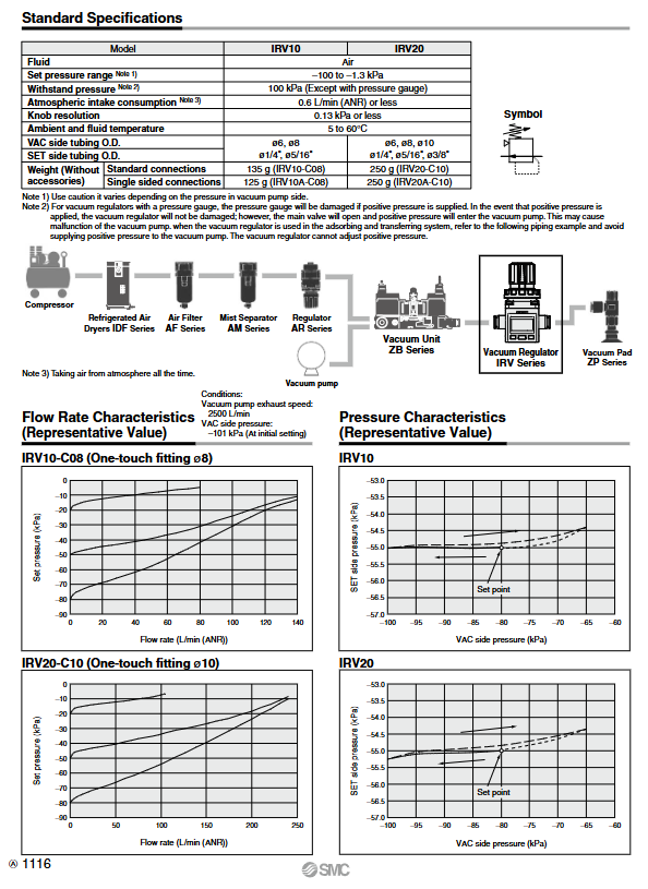
Brand and positioning: The IRV10/20 series vacuum regulator launched by SMC is positioned as a precise pressure control equipment for industrial vacuum systems, with three major advantages of high flow rate, lightweight, and flexible installation. It is suitable for vacuum adsorption, leak testing, and other scenarios. It is an upgraded version of the previous generation IRV1000/2000 series, with a weight reduction of 20% and a flow rate increase of over 2 times.
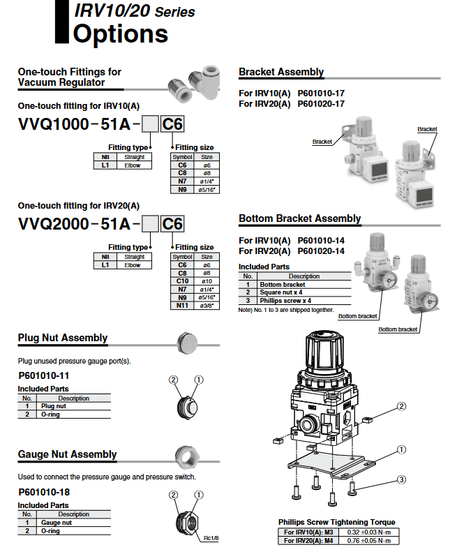
Quick change connector: Built in straight/curved quick change connector, IRV10 (A) compatible with VVQ1000 series, IRV20 (A) compatible with VVQ2000 series, supports switching between straight (Nil logo) and curved (L/L1 logo).
Installation bracket: Optional ordinary bracket (B label), bottom bracket (L label), IRV10 (A) bracket model P601010-17, IRV20 (A) bracket model P601020-17; The bottom bracket includes the bracket body, 4 square nuts, and 4 cross screws. The tightening torque of the screws is: IRV10 (A) (M3) 0.32 ± 0.03 N · m, IRV20 (A) (M4) 0.76 ± 0.05 N · m.
|Identification | Output Specification | Supporting Model | Functional Features|
|ZN | NPN collector open circuit 1 output | ZSE20-N-M-01-L | Lead length 2m, with connector|
|ZP | PNP collector open circuit 1 output | ZSE20-P-M-01-L | Lead length 2m, with connector|
|ZA | NPN collector open circuit 2 output+replication function | ZSE20A-X-M-01-J | Lead length 2m, with connector|
|ZB | PNP collector open circuit 2 output+copy function | ZSE20A-Y-M-01-J | Lead length 2m, with connector|
Core parameters: applicable pressure range 0.0~-101.0kPa, minimum set increment 0.1kPa, power supply 12-24VDC, current consumption ≤ 35mA, maximum load current 80mA.
Working principle and structural design
Working Principle:
Pressure regulation: Rotate the knob clockwise, adjust the spring to push the diaphragm and valve, connect the VAC side (vacuum pump) and SET side (load), and increase the vacuum degree on the SET side; The pressure on the SET side is transmitted to the vacuum chamber through the airway and balanced with the spring force to achieve pressure stability.
Pressure compensation: When the vacuum degree on the SET side is higher than the set value, the diaphragm moves upward, the valve closes, and the atmospheric suction valve opens to supplement the atmosphere and reduce the vacuum degree; When the vacuum degree on the SET side is lower than the set value, the diaphragm moves down, the atmospheric suction valve closes, and the valve opens to increase the vacuum degree.
Structural design:
Core components: knob (with locking function, press the hidden orange ring to lock), regulating spring, atmospheric suction valve, vacuum chamber, diaphragm, valve stem, valve.
Fixed method: The pressure gauge/digital pressure switch is fixed with a clip buckle. When disassembling, the clip must be removed first, and pressure operation is prohibited; The quick change connector is designed in a cartridge style and secured with a clip. To replace it, a Phillips screwdriver is needed to remove the clip.
Protective design: Airway aperture ø 2.6mm to avoid blockage; The side air intake holes of the fuselage need to be kept unobstructed, otherwise the pressure cannot be adjusted normally.
Ordering rules and customization options
Standard ordering code structure:
Standard connector: IRV+body size (10/20)+connector type (Nil=straight, L=curved)+pipe diameter symbol (e.g. C08=ø 8mm)+accessory symbol (e.g. G=pressure gauge, ZN=digital pressure switch)+installation accessories (e.g. B=bracket)
Single side connection model: IRV+body size (10/20)+A (single side connection)+joint type+pipe diameter symbol+accessory symbol+installation accessories
Example: IRV20A-L-C08-ZB-B (IRV20 single-sided connection, curved joint, ø 8mm pipe diameter, PNP dual output digital pressure switch, with bracket)
Customization option: Panel installation integrated digital pressure switch (selection symbol X1), please contact SMC to confirm detailed dimensions, specifications, and delivery cycle. The maximum thickness of the compatible panel is 3mm for IRV10A and 4mm for IRV20A.
Installation and usage specifications
Installation points:
Pipeline connection: VAC port connected to vacuum pump, SET port connected to load, reverse connection is prohibited; Attention should be paid to the VAC/SET side direction for single-sided connection models, and the pressure gauge/pressure switch should be inserted in place (with the nut flush with the product surface).
Environmental requirements: Avoid corrosive gases, dust, vibration, direct sunlight, and heat source radiation; The dust environment requires the installation of a vacuum filter or drainage separator at the SET port.
Pressure limit: The model with a pressure gauge is prohibited from using positive pressure, otherwise it may damage the pressure gauge; The flow rate of the vacuum pump needs to be matched, and when the flow rate is insufficient, an air storage tank can be added on the VAC side.
Operation taboos:
When under pressure, it is forbidden to disassemble the screws, valve guides, or pressure gauges/switches of the machine body. The set pressure should be adjusted to 0 (atmospheric pressure) first and the vacuum pump should be turned off.
Do not block the side air inlet of the aircraft; When inserting the curved quick change connector into the pipeline, the connector should be held by hand to avoid leakage or damage caused by force.
Maintenance instructions:
Vulnerable parts: diaphragm components (IRV10: P6010-2; IRV20: P601020-2), valve components (IRV10: P6010-3; IRV20: P601020-3), all made of materials such as HNBR.
Cleaning requirements: Use only non corrosive cleaning agents for wiping, and do not use solvent based products.