WESTINGHOUSE iGen5000 Digital Inverter Generator
Product Overview and Core Parameters
Category specific specifications
Power parameters: Rated operating power: 3900W; Peak power: 5000W
Electrical characteristic voltage: 120V; frequency: 60Hz; phase: single-phase; Total harmonic distortion ≤ 3%
Power configuration: Engine displacement: 224cc; Spark plug model: 97109-F7RTC; Spark plug clearance: 0.60-0.80mm
Capacity specification: Fuel tank capacity: 3.4 gallons (12.8 liters); Oil capacity: 0.63US qt (0.60 liters)
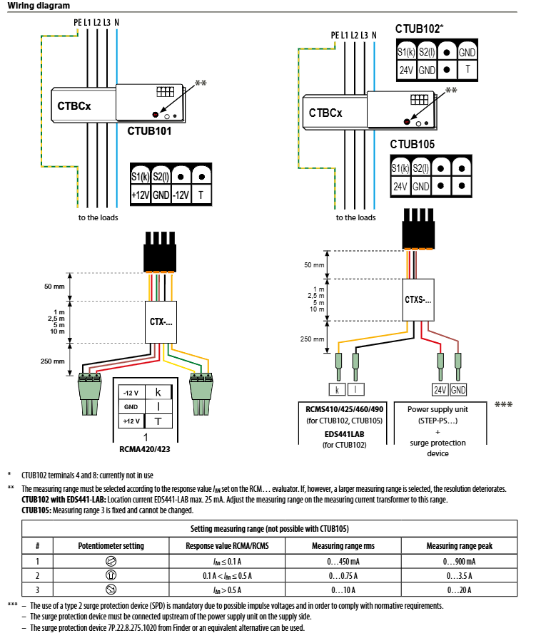
Remote start (up to 30 meters), electric start, manual start
Core Design: Digital Voltage Regulator, Permanent Magnet Generator, Floating Neutral Grounding System
Physical parameter protection level IP20/NEMA 1; Working temperature: -10~+50 ℃; Storage temperature: -20~+70 ℃
Core functions and operations
(1) Core functions
Operation mode: ECO energy-saving mode can adjust the engine speed according to the load, reducing fuel consumption and noise; Non ECO mode is suitable for high-power devices such as air conditioning and water pumps.
Output interface: including 120V 20A NEMA 5-20R dual socket, 120V 30A NEMA TT-30R socket, dual USB 5V/2.1A interface, to meet the simultaneous power supply of multiple devices.
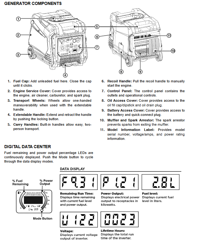
Digital data center: Real time display of remaining operating time, output power (kW), fuel level (liters), voltage, and cumulative operating hours.
Parallel operation: Connect generators of the same model through dedicated parallel cables (to be purchased separately) to increase total power output. Parallel operation is not supported in ECO mode.
(2) Operation process
Preparation before startup: Add 87-93 unleaded gasoline (ethanol content ≤ 10%, E15/E85 prohibited), check the oil level, ensure the load is disconnected, and confirm that the equipment is placed outdoors in a dry and flat area (at least 5 feet away from doors and windows).
Startup steps: Turn on the fuel switch → Turn on the battery switch → Select the startup mode (remote control press for 1 second/electric start press for 2 seconds/manual start) → Wait for the “output ready” LED to light up → Connect the load (in the order of “high power priority”).
Shutdown steps: Disconnect all loads → Run without load for a few minutes → Press the shutdown button/remote control to stop → Turn off the battery switch and fuel switch.
Safety standards and protection mechanisms
(1) Safety usage requirements
It must be used outdoors in a well ventilated area. It is strictly prohibited to operate in enclosed spaces such as indoors, garages, and basements to avoid carbon monoxide poisoning. It is recommended to equip a carbon monoxide detector.
Avoid use in damp environments, prevent rainwater and spray from contacting equipment, as damp environments can easily cause short circuits and electric shocks.
Maintain a ventilation gap of 5 feet around the equipment, keep away from combustibles, and have the exhaust outlet facing the unmanned area.
Before refueling, it is necessary to stop the machine and cool it down for 5 minutes. Smoking or approaching open flames are prohibited to avoid fuel spillage.
(2) Multiple protection functions
Protection type triggers condition protection action
Overload protection cuts off AC output when the output current exceeds the rated value, and the overload LED lights up
Low oil level protection: If the oil level is below the safety threshold, the machine will automatically shut down and the low oil LED will light up
Overcurrent protection: When the current exceeds 200% of the rated value, the output is immediately cut off
Overvoltage/undervoltage protection 230V input:>410VDC/<190VDC; 460V input:>810VDC/<380VDC Cut off output to avoid equipment damage
Grounding fault protection detection triggers protection shutdown due to abnormal grounding
Overheating protection: The engine or inverter will automatically shut down and cool down if the temperature is too high
Maintenance and Storage
(1) Regular maintenance cycle and project
Core projects of maintenance cycle
Check the oil level, fuel level, cable and socket status before each use
First 25 hour/1 month engine oil change
Change engine oil and clean air filter every 50 hours/6 months
Clean spark plugs and spark arresters, check fuel filters, and adjust valve clearances every 100 hours/6 months
Replace spark plugs, air filters, and fuel filters every 300 hours/year
(2) Storage requirements
Storage duration operation requirements
No special treatment required for less than 1 month, keep the fuel tank sealed
Add fresh gasoline and fuel stabilizer every 2-6 months, and empty the carburetor float chamber
Drain the fuel tank and carburetor, inject a small amount of oil into the cylinder, and disconnect the battery connection for at least 6 months
Common troubleshooting
Common causes and solutions for fault phenomena
Unable to start battery shutdown, low fuel, wet/faulty spark plug, clogged air filter to open battery, refuel, dry/replace spark plug, clean air filter
Shutdown after startup due to low fuel level, fuel contamination, clogged air filter, oil replenishment, replacement of fresh fuel, and cleaning of air filter
No output power overload triggering protection, circuit breaker tripping, load fault disconnecting load, resetting circuit breaker, checking load equipment
Insufficient power, poor fuel quality, clogged air filter, unadjusted fuel replacement at high altitude, clean air filter, installation of high-altitude carburetor kit (>2000 feet)