Core positioning: Universal programmable controllers (PCs) that support full scenario industrial automation requirements from simple conditional control to complex arithmetic control, and can simultaneously execute ladder diagrams, HI-FLOW, and C language programs.
Application restrictions: Not recommended for high security responsibility scenarios (such as power plant control, medical equipment, traffic signal systems, etc.), unless approved by Hitachi and configured with redundant design.
Compliance requirements: Exports must comply with relevant restrictions such as Japan’s Foreign Exchange and Foreign Trade Act and US export control regulations.
Core components and specifications of the system
(1) Core hardware components
Component Type Key Model Core Parameter Function Description
The CPU module LQP600 has a maximum of 2048 I/O points and 3100mA current consumption. It is the core control unit of the system and supports multi language programming execution
The power module LQV410 inputs 100-120VAC/100-110VDC and outputs 5VDC/10A to provide stable power supply for the system, with overcurrent (OC) and overvoltage (OV) protection
The RI/O-IF module LQE950 has 2 remote I/O lines and a communication rate of 768kbps to achieve remote I/O communication expansion, supporting up to 12 PI/O units cascaded together
The option modules OD. RING (LQE510-E), ET.net (LQE260-E), etc. support protocols such as FL net and Ethernet to extend network communication and data sharing functions
PADT is a dedicated computer terminal compatible with Windows 7/10 (64 bit) with a CPU of 1GHz or above and 2GB or more of memory for programming, debugging, and monitoring systems
(2) Key system specifications
Environmental parameters: operating temperature 0-55 ° C, storage temperature -20-75 ° C, relative humidity 10-90% RH (non condensing), seismic grade in accordance with JIS C 60068-2-6, impact resistance grade in accordance with JIS C 60068-2-27.
Performance indicators: Maximum I/O points of 2048, maximum transmission distance of remote I/O single channel of 300m (up to 3.3km after optical adapter expansion), communication protocol support for IEEE802.3i/802.3u (Ethernet), FL net, DeviceNet, etc.
Physical specifications: The weight of the 7-slot mounting base (HSC-1770) is ≤ 1300g, the weight of the CPU module is ≤ 450g, and the tightening torque of the module mounting screws is 1.0N · m.
Safety regulations and operational requirements
(1) Safety warning classification
DANGER: Fatal risk (such as electric shock caused by ungrounded), it is necessary to ensure that the protective grounding terminal is reliably grounded.
Warning: Serious risks (such as electric shock/fire caused by live plugging and unplugging modules), the power must be turned off before module installation/removal.
CAUTION: Minor injury risk (such as injury caused by foreign objects entering the module gap), it is prohibited to block the module ventilation duct.
Notice: Property damage risk (such as module failure caused by static electricity), human static electricity must be released before contacting the equipment.
(2) Core security operations
Power operation: The input voltage should not exceed the rated value, and fuses should be installed on both sides of the AC power supply to avoid component damage caused by overcurrent/overvoltage.
Module insertion and removal: All modules must be powered off before installation/removal, and live operation is prohibited to prevent electric shock or equipment damage.
Battery usage: The main battery (HDC5200) is prohibited from charging, heating, or short circuiting. The replacement cycle is ≤ 5 years, and it should be disposed of as industrial waste.
Grounding requirements: It must comply with Class D grounding standards (grounding resistance ≤ 100 Ω), avoid sharing the grounding main line with AC panels, and have a spacing of ≥ 15m.
Installation and operation process
(1) Key installation requirements
Installation gap: The distance between the cabinet and the unit should be ≥ 100mm, and the distance between the sides should be ≥ 50mm to ensure natural heat dissipation. The intake temperature should not exceed 55 ° C.
Grounding installation: The cabinet needs to be welded to the steel frame of the building or a separate grounding electrode. When multiple cabinets are installed, a chrysanthemum connection grounding method is used.
Module assembly: The installation base needs to be fixed on the vertical surface of the cabinet, and the modules need to be installed in dedicated slots (PS slot, CPU slot, etc.), with screws tightened to avoid loosening.
(2) Debugging and operation tools
Core tool: BASE SYSTEM/s10VE, supports project creation, network configuration, program download, fault diagnosis and other functions, requires administrator privileges for installation.
Backup and Recovery: Supports CPU data backup, recovery, and backup data comparison. Backup files include main memory and MRAM data. When restoring, ensure that the CPU is in STOP mode.
Troubleshooting: Locate faults through LED indicator lights (RUN/ERR/STBY/ALARM) and error logs, support remote reset, module list viewing, performance monitoring, and other functions.
Product identity: ABB’s fifth generation synchronous equipment (SYNC HROTACT) ® 5) Specially designed for the synchronization and parallel connection of synchronous motors with the power grid and synchronous lines.
Core function: Ensure the safety of parallel operation in the power system, and avoid problems such as grid disturbance, circuit breaker tripping, and equipment damage caused by asynchronous voltage at both ends.
Application Scenario:
Power station: parallel connection of generator and power line
Substation: Two synchronous lines connected in parallel
Supports manual/fully automatic operation mode, can be used as an independent synchronization unit or monitoring element (Synchrocheck)
Security and usability design
Key configuration principle:
Dual channel: Two channels are connected in series, monitoring each other, blocking fault operations, and improving safety (hardware/software independent design, different microprocessors, avoiding systematic failures)
Redundancy design: Two devices connected in parallel, automatically switching in case of failure, improving system availability
Automatic single channel+manual parallel switch parallel+series synchronization check (SYN 5201)
Redundant dual channel system (SYN 5302, highest security and availability)
Core functions and features
Specific content of functional categories
Parameter storage single device supports 7 sets of parameters and adapts to 7 different parallel points
Frequency adaptation compatible with rated frequencies of 50 Hz, 60 Hz, and 16 ²/³ Hz
Hardware features: Digital I/O can be freely configured; Output contacts carry higher current, reducing the need for auxiliary relays; All I/O isolation; No need for independent power supply
Debugging convenience: 1. Support SynView software debugging, automatically recommend parameters and label extreme/default values; 2. It can be manually debugged through the device panel without the need for a PC. 3. The intelligent program can recommend parameters based on the characteristics of the generator
The system integration supports bus protocols such as IEC 61850, MODBUS RTU, Profibus DP, LON Bus, etc., making it easy to integrate into modern control systems
Remote maintenance is equipped with Ethernet interface (TCP/IP protocol), which is assigned with independent IP, and can be remotely accessed and debugged through the Internet
Compatibility can be retrofitted with previous generation SYNC HROTACT systems or other manufacturers’ synchronous devices
Product model classification and core parameters
Model Product Type Installation Method Key Dimensions (W × H × D) Weight
SYN 5100 Simple Synchrocheck Guide Rail Buckle Installation 205 × 128 × 82 mm 0.3 kg
SYN 5200 Advanced Function Synchronization Inspector Panel Installation 221 × 163 × 220 mm 4.0 kg
SYN 5201 single channel automatic synchronization equipment (including frequency and voltage regulation) panel installation 221 × 163 × 220 mm 4.0 kg
SYN 5202 Dual Channel Automatic Synchronization System (Serial Synchronization Check) Panel Installation 221 × 163 × 220 mm 4.0 kg
SYN 5302 Redundant Dual Channel Automatic Synchronization System Panel Installation 442 × 154 × 220 mm 8.0 kg
SYN 5500 multi parallel point connection auxiliary equipment rail buckle installation 381 × 128 × 50 mm 1.4 kg
Technical standards and compliance
EMC (Electromagnetic Compatibility) standard:
Conducted emission: CISPR 22 Class B; Radiation emission: CISPR 11 Class A Group 1
Immunity: Complies with IEC 61000-4 series (electromagnetic fields, fast transients, surge voltages, etc.), IEC 60255-22-1 (1 MHz pulse disturbance 2.5 kV)
Compliance Directive:
LV Directive: 73/23/ECC (compliant with EN 60950)
Electromagnetic Compatibility Directive: 89/336/ECC (compliant with IEC 61000-6-4/6-2)
Type: YASKAWA Direct Drive Servo System Product Manual
Core objective: To provide selection, technical parameters, system construction, and wiring guidance for motors and amplifiers, and to assist in the integration of high-precision equipment
Series power supply specifications adapted to motor capacity control function core parameters
SGDS single-phase 100V/200V small capacity (2-35N · m) position/speed/torque control, electronic gear continuous output current 2.1-11.6Arms
SGDH single-phase/three-phase 200V full capacity (2-200N · m) with SGDS function+self-tuning, harmonic suppression continuous output current 2.1-24.8Vrms
Model interpretation (taking SGDS-02A01A as an example):
02: Suitable for 0.2kW motor; A: 200V power supply; 01: Standard interface (analog voltage/pulse)
Control performance: speed control range 1:5000, load regulation rate ± 0.01% (rated speed), torque control repeatability ± 1%
Input/output: Analog reference ± 1-10V, maximum pulse frequency 1Mpps (line drive), I/O signal supports custom allocation
Protection function: multiple protections such as overcurrent, overvoltage, undervoltage, overload, encoder error, etc
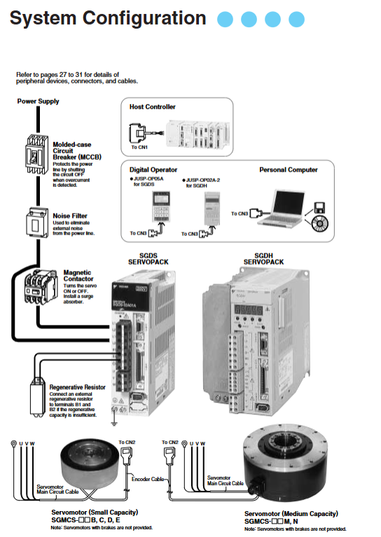
System configuration and wiring
1. Core component configuration
Power supply circuit: MCCB (molded case circuit breaker) → noise filter → electromagnetic contactor → amplifier
Signal circuit: host controller → amplifier CN1 (I/O) → motor CN2 (encoder)
Peripheral accessories: Regenerative resistor (when regenerative energy is insufficient), DC reactor (to suppress harmonics), surge absorber
2. Key wiring requirements
Main circuit: The U/V/W phase line of the motor corresponds to the amplifier output terminal, and the FG terminal must be grounded (grounding resistance ≤ 100 Ω)
Encoder: Shielded twisted pair cable, maximum distance of 50m, single ended grounding of shielding layer
Control circuit: Shielded twisted pair cables are used for I/O signals, with a distance of ≥ 30cm from the main circuit to avoid interference
3. Typical wiring diagram
Single phase 200V (SGDS): L1/L2 connected to single-phase power supply, B1/B2 connected to regenerative resistor, CN2 connected to encoder, CN1 connected to control signal
Three phase 200V (SGDH): L1/L2/L3 connected to three-phase power supply, 1/2 terminal connected to DC reactor, other interfaces consistent with single-phase
Selection and peripheral devices
1. Selection process
Determine load torque/speed → Select motor model (by outer diameter/torque)
Select amplifier (SGDS/SGDH) based on motor capacity/power supply type
According to system requirements → configure peripheral devices (filters, reactors, cables)
2. Selection of commonly used peripheral devices
Example of Equipment Type and Model Applicable Scenarios
Noise filter FN2070-6/07 suppresses power side noise and is suitable for 200W motors
DC reactor X5054 suppresses harmonics and is compatible with SGDS series
Digital Operator JUSP-OP05A Amplifier Parameter Configuration/Monitoring
Encoder cable JZSP-CMP60-05 motor amplifier encoder connection (5m)
Main circuit cable JZSP-CMM60-03 motor amplifier power connection (3m)
Core objective: To guide professional technicians to complete the safe installation, wiring, parameter configuration, trial operation, and fault handling of frequency converters
Applicable restrictions: limited to industrial motor control only, not used in special fields such as life support systems, nuclear industry, etc
Safety regulations (core focus)
1. Definition of risk level
Typical scenarios of risk level meaning
DANGER may cause death/serious injury due to live wiring and non discharge of internal capacitors during operation
Warning: May cause death/serious injury. Flammable materials near frequency converter, poor grounding
CAUTION may cause minor/moderate injury when touching high-temperature heat sinks or handling unsecured cover plates
NOTICE may cause equipment damage due to unused shielded wires and withstand voltage testing
2. Key safety requirements
Electrical safety: Power off before wiring, wait for capacitor discharge (indicator light off, DC bus voltage<50Vdc); Grounding resistance: 200V level ≤ 100 Ω, 400V level ≤ 10 Ω
Mechanical safety: Models weighing ≥ 15kg require 2 people and lifting equipment for handling, and it is prohibited to grip the front cover/terminal cover
Operation safety: Remove the motor load before Auto Tuning; 3-wire control needs to set b1-17=0 (ignore RUN command when powered on)
Installation specifications
1. Mechanical installation
Installation direction: Priority should be given to vertical installation (to ensure heat dissipation), special models can be installed on the side (please consult the manufacturer)
Distance requirement:
Single machine: Up and down ≥ 120mm, left and right ≥ 30mm, front ≥ 50mm
Side by side installation (specific model): Drive spacing ≥ 2mm, L8-35=1 needs to be set
Environmental restrictions:
Temperature: Open type (IP20) -10~50 ℃, Closed type (UL Type 1) -10~40 ℃
Altitude: ≤ 1000m (over 1000m, capacity reduction of 1% per 100m)
Main circuit power line cross-section ≥ 0.75mm ² (control circuit), tightening torque 3.6-41.5N · m R/L1/S/L2/T/L3 (input), U/T1/V/T2/W/T3 (output)
Control circuit shielded twisted pair cable, up to 3m in length, with a distance of ≥ 30cm from the power line S1-S8 (multifunctional input), A1-A3 (analog input), FM/AM (analog output)
The grounding terminal on the motor side must be grounded, and the shielding layer must be grounded at one end FG (driver grounding) and the motor casing must be grounded
Control mode parameter setting applicable scenarios core advantages
V/f control A1-02=0 fan, pump, multi motor linkage has strong universality and does not require motor parameters
Open loop vector (OLV) A1-02=2 high-precision speed control without speed feedback, high low-speed torque
EZ vector A1-02=8 simplified settings for ordinary variable speed scenarios, no need for fine tuning
Troubleshooting
1. Common faults and solutions
Fault code, fault name, common causes, and solutions
Check the wiring for overcurrent output short circuit, heavy load, and short acceleration time at oC, reduce load, and increase C1-01
OV overvoltage deceleration time is too short, brake resistor damage increases deceleration time, replace brake resistor, activate L3-04 (stall prevention)
Overloading of oL1 motor, overload of motor, low speed to reduce load, use of forced cooling motor, correction of E2-01 parameters
Overload of oL2 drive, insufficient drive capacity, low-speed high torque replacement with large capacity models, reducing load
GF grounding fault output side grounding short circuit, motor insulation damage inspection wiring, testing motor insulation resistance (≥ 10M Ω)
STo safety torque OFF safety input terminal disconnection inspection H1/H2/HC wiring, reset safety controller
2. Fault reset process
Remove the source of the fault (such as power-off inspection of wiring, reducing load)
Waiting for the discharge of the driver capacitor (indicator light off)
Press the RESET key on the keyboard, or power off and restart
If it repeatedly occurs, check the parameter configuration or contact the manufacturer for repair
Compliance and scrapping
Compliance standards: Complies with IEC/EN 61800-5-1, UL 508C, CSA C22.2 No.100
Scrap requirements:
Separate the battery (CR2016) and microSD card and dispose of them separately according to regulations
SD cards need to be physically destroyed or data erased to prevent information leakage
Drive body is classified and recycled according to industrial waste
Type: YASKAWA ∑ – V Series AC Servo Drive User Manual (Design and Maintenance)
Applicable products: SERVOPACK (SGDV series)+servo motor (rotary type: SGMMV/SGMJV, etc.); Direct Drive Type: SGMCV/SGMCS
Core objective: To guide the entire process of product design, testing, adjustment, and maintenance, and meet the requirements of high-frequency, high-speed, and high-precision positioning
SGLF F-type iron core with high thrust density, supporting self cooling/water-cooled medium and heavy-duty automation equipment
SGLT T-shaped iron core vigorously promotes heavy-duty machine tools and large-scale production lines
Model interpretation: Taking SGLFW2-30A070AS1 as an example, “SGL” is the ∑ -7 series identifier, “F” is the F-type iron core, “W2” is the rotor, “30” is the magnet height of 30mm, “A” is powered by 200V, “070” is the rotor length of 70mm, “AS” is with polarity sensor and thermal protector, and “1” is the self cooling method.
2. Core performance parameters
Power supply voltage: uniformly 200VAC (single-phase/three-phase), insulation level B, withstand voltage 1500VAC/1 minute
Thrust range: rated thrust 0.1-2520N, instantaneous maximum thrust 30-7560N
Speed range: rated speed 0.5-5m/s, maximum speed 1.5-7.5m/s
Environmental requirements: working temperature 0-40 ℃, humidity 20% -80% RH (non condensing), altitude ≤ 1000m
Selection calculation
1. Core formula for selection
Steady state thrust:F L=9.8×M×(m W+m T+m M)+F(m Acceleration thrust:F P=(m W+m T+m M)× t onev+F L (v is speed, t ₐ is acceleration time)
Effective thrust:F RMS= tF Ptwo⋅t one+F L two⋅t C+F S two⋅t d(t is the cycle time)
2. Selection verification criteria
Acceleration thrust ≤ maximum thrust × 0.9
Effective thrust ≤ rated thrust × 0.9
Load quality ≤ maximum allowable load (to be combined with brake resistor configuration)
Installation specifications
1. Installation environment requirements
Environmental restrictions: Indoor use, no corrosive/explosive gases, no strong magnetic field interference
Special protection: The magnetic track contains strong permanent magnets and should be kept away from electronic medical equipment such as pacemakers to avoid magnetic substances from approaching
2. Installation operation process
(1) Magnetic track installation
Positioning accuracy: magnetic track spacing tolerance ± 0.1mm, alignment with reference marks when connecting multiple magnetic tracks
Fixed requirement: Use grade 10.9 hex screws with a tightening torque of 3.6-41.5N · m (depending on the model)
Gap control: The gap between the magnetic track and the rotor is 0.8-1.4mm (0.5-1.2mm with magnetic cover)
(2) Assembly of moving parts
Installation steps: First fix the rotor to the workbench → slowly approach the magnetic track → confirm that there is no contact noise → calibrate the gap with a non-magnetic feeler gauge
Flow pressure: rated flow 4L/min, maximum pressure 0.5MPa, water temperature 5-25 ℃
Protective measures: The pipeline needs to be made of stainless steel material and equipped with a filter (to filter impurities ≥ 0.5mm)
Connection configuration
1. Linear encoder connection
Compatible brands: Supports mainstream brands such as Heidenhain, Renishaw, Mitutoyo, etc
Installation conditions: The distance between the magnetic track and the magnetic track should be ≥ 10-40mm (depending on the motor model) to avoid magnetic leakage interference
Adjustment requirements: The exposed encoder needs to calibrate the position of the scanning head, and the sealed encoder needs to meet the installation tolerance
Recommended models for cable type length restrictions
Servo main circuit cable ≤ 20 meters JZSP-CLN11/21/39 series
Encoder cable ≤ 50 meters JZSP-CLL00/30 series
Sensor cable ≤ 15 meters JZSP-CLL10/CL2L100 series
Grounding requirements: The grounding resistance of the servo amplifier should be ≤ 10 Ω (400V level)/≤ 100 Ω (200V level), and the shielding layer should be grounded at one end
3. Serial Conversion Unit (JZDP Series)
Function: Convert encoder signal to servo amplifier, support polarity sensor and thermal protector signal transmission
Key parameters: Power supply+5V ± 5%, current consumption ≤ 160mA, operating temperature 0-55 ℃
Maintenance and disposal
1. Regular inspection
Daily inspection: Check for vibration, abnormal noise, and cable wear daily to confirm that screws are not loose
Regular inspection: calibrate the gap between the magnetic track and the rotor annually, measure the insulation resistance (≥ 10M Ω/500VDC)
Overhaul cycle: Contact the manufacturer for comprehensive maintenance every 5 years, and do not disassemble on your own
2. Key points for troubleshooting
Common problems: Abnormal encoder signal (check installation spacing), overload alarm (verify effective thrust), cable breakage (check bending radius)
Insulation testing: Measure after disconnecting the servo amplifier, and do not perform voltage withstand testing on the sensor
3. Scrap disposal
Demagnetization requirement: The magnetic track needs to be heated to above 300 ℃ and maintained for 1 hour to eliminate magnetism
Environmental requirements: Follow the WEEE directive and classify the disposal of electronic components and metal casings
Safety and Compliance
1. Core security standards
Strong magnetic protection: The magnetic track has an adsorption force of up to 21500N, and non-magnetic tools should be used during operation to avoid finger squeezing
Power off operation: Disconnect the power before maintenance and wait for the servo amplifier CHARGE indicator light to turn off (≥ 5 minutes)
Static protection: Release static electricity before touching the connector, and do not directly touch the encoder pins with your hands
2. Compliance standards
North America: UL 1004-1, UL 1004-6, CSA C22.2 No.100
EU: CE certification (EMC 2014/30/EU, LVD 2014/35/EU), EN 61800-3
China: RoHS compliance, restricting harmful substances such as lead and mercury
Product Name: YASKAWA GA500 Series AC Micro Drives for Industrial Applications
Model identification: CIPR-GA50Cxxxxxxxx, core specifications are classified as follows:
Voltage level, input type, power range, key parameters
200V single-phase 0.1-4.0 kW Max
200V C three-phase 0.1-22kW speed control range 1:40~1:100
400V level three-phase 0.37-30 kW protection level IP20/UL open type
Core features: Supports 5 control modes, compatible with induction motors, PM motors (including IPM/SPM), and synchronous reluctance motors (SynRM), with functions such as automatic tuning, energy saving, and dynamic braking.
2. Definition of core terms
Key abbreviations: OLV (open-loop vector control), PM (permanent magnet synchronous motor), MFAI (multifunctional analog input), MFDO (multifunctional digital output), ND (normal load), HD (heavy load)
Environmental conditions: Indoor use, pollution level 2, altitude ≤ 1000m (with a 1% reduction in capacity for every 100m exceeding 1000m), vibration ≤ 1G (10-20Hz)/0.6G (20-55Hz)
Installation gap: Single driver up and down ≥ 100mm, left and right ≥ 30mm; for parallel installation, L8-35=1 should be set, and for horizontal installation, some models require an external cooling fan (such as B001-B012, which requires a 0.18m ³/min air flow fan)
Disassembly and assembly operation: The front cover/keyboard requires a specified size screwdriver (blade width ≤ 2.5mm) to avoid touching the internal capacitors (after power failure, wait for voltage ≤ 50Vdc)
Wire specifications: Recommended 2.5mm ² for 200V single-phase B001 model, 25mm ² for 400V three-phase 4060 model, tightening torque 0.5-5.5N · m (depending on terminal size)
Control circuit wiring:
Signal mode: MFDI supports Sink/Source mode, switched through SC-SP/SC-SN jumper
Wiring requirements: Shielded twisted pair, length ≤ 50m, distance from main circuit ≥ 30cm, to avoid electromagnetic interference
Startup and Debugging Process
1. Operation preparation
Parameter settings:
General setting mode (SrUP): including 26 core parameters such as control mode (A1-02), acceleration and deceleration time (C1-01/C1-02), motor parameters (E2-01~E2-04), etc
Application preset (A1-06): Automatically optimize parameters for specific scenarios, requiring initialization (A1-03=2220/3330)
Keyboard operation: Supports LOCAL/EMOTE switching, RUN/STOP keys (STOP key priority can be disabled through o2-02), can backup/restore parameters (o3-01)
2. Auto Tuning
Tuning type:
Applicable scenarios for motor type tuning method parameter settings
Induction motor rotation tuning T1-01=0. The motor can disconnect from the load and requires a no-load rate of ≥ 30%
Induction motor static tuning T1-01=1 motor cannot rotate, load ≤ 30%
PM motor rotation tuning T2-01=4 needs to disconnect the load and automatically detect motor parameters
PM motor static tuning T2-01=1 motor fixed, suitable for non rotating scenarios
Prerequisite: Enter the motor nameplate parameters (rated power, voltage, current, number of poles), disable safe disable input during tuning, and avoid personnel approaching rotating parts.
3. Test Run
No load test: Start at a frequency of 6Hz, gradually increase to the rated frequency, and check the motor direction, vibration, and current (≤ rated current)
Load testing: Verify acceleration/deceleration response and torque output, fine tune parameters through C4-01 (torque compensation) and n1-02 (anti oscillation gain)
Checklist: Confirm power supply voltage, wiring correctness, protection parameters (L1-01 motor overload protection), and control signal effectiveness
Standard Compliance and Safety
1. Main compliance standards
EU CE: Complies with LVD (2014/35/EU), EMC (2014/30/EU), Machinery Directive (2006/42/EC), requires the use of built-in EMC filters (model suffix E) and proper grounding
UL in the United States and Canada: Compliant with UL 61800-5-1, branch circuit protection requires designated fuses (such as FWH-25A14F for B001), and control circuits require UL certified Class 2 power supply
China RoHS: Restricting harmful substances such as lead and mercury, providing a list of hazardous substances
2. Core safety requirements
Electrical safety: Wait for at least 5 minutes after power failure, prohibit live wiring/cover removal, grounding wire cross-section ≥ 10mm ² (copper core)
Mechanical safety: It is prohibited to grip the keyboard/front cover during lifting, the installation area should be free of flammable materials, and the emergency stop circuit should be independent of the frequency converter
Functional safety: Safe Disable input (H1/H2/HC) requires Source mode, with a wiring length of ≤ 30m
Operation and maintenance
1. Network communication
Supporting protocol: MEMOBU/Modbus (RS-485), with a maximum baud rate of 115.2kbps, supports master-slave configuration, and can communicate with PLC
Communication settings: The terminal resistor is enabled through DIP switch S2, and the last slave needs to be set to ON. The message format includes address, function code, and data segment
2. Troubleshooting
Common faults: OV (overvoltage), oL1 (motor overload), STPo (motor out of step), oC (overcurrent)
Troubleshooting process: After the fault occurs, power off for cooling, check the wiring → parameter settings → load status → motor insulation, and monitor the operating data (output frequency/current/voltage) through U1 xx
3. Maintenance and disposal
Regular inspection: daily (operation status, abnormal noise), regular (cooling fan replacement, 2-5 years according to model), storage (-20~70 ℃, moisture-proof)
Scrap requirements: Follow the WEEE directive, classify and dispose of electronic components and metal casings, and prohibit the indiscriminate disposal of oil/hazardous substance containing components
Summary of Key Parameters
Parameter Category Core Parameters Default Values Adjustment Range Usage
Control mode A1-02 0 (V/f) 0-8 Select control mode (V/f/OLV/PM, etc.)
Motor protection L1-01 according to A1-02 0-6 motor overload protection type (constant torque/variable torque)
Acceleration and deceleration time C1-01/C1-02 1.0 0.01-3600 years adjustment start/stop smoothness
Carrier frequency C6-02 1 (2kHz) 1- Upper limit balanced motor noise and heat dissipation
This document is the Spanish technical manual (manual number TOSP C710606 22B) for the Yaskawa V1000 series vector controlled compact frequency converter (model CIMR-VU), covering 200V single/three-phase (0.1-18.5kW) and 400V three-phase (0.2-18.5kW) models. The core provides guidance around the entire life cycle of the equipment, including receiving inspection, mechanical/electrical installation, programming start-up, troubleshooting, regular maintenance, peripheral equipment adaptation and other key contents. It emphasizes safe operation norms and precise parameter configuration, supports the control of ordinary induction motors and permanent magnet synchronous motors (PM), and provides comprehensive technical support for installation, commissioning, daily operation and maintenance, and fault resolution in industrial scenarios.
Detailed analysis of core chapters
Basic Information and Security Principles of Documents
Basic Information
Product positioning: Vector controlled compact frequency converter, suitable for 7 typical industrial applications such as pumps, conveyors, fans, compressors, cranes, etc.
Voltage and power range: 200V single-phase (0.1-5.5kW), 200V three-phase (0.1-18.5kW), 400V three-phase (0.2-18.5kW).
Document purpose: To guide users in correctly installing, operating, and maintaining equipment, and to clarify that users need to pass on the manual to the end user.
Copyright Notice: All rights reserved by Yaskawa Electric in 2008. Reproduction and dissemination are prohibited without written permission. Product information may change with upgrades, and we do not assume any responsibility for losses caused by misuse of information.
General Safety Principles
Security level definition: divided into four levels: “PELIGRO (fatal danger)”, “ADVERTENCIA (serious danger)”, “PRECAUCI Ó N (minor injury)”, “AVISO (property damage)”, clarifying the warning requirements for different risk scenarios.
Core safety regulations: After power failure, wait for ≥ 5 minutes for capacitor discharge (bus voltage<50Vdc); Prohibit live wiring or touching circuit boards; Only qualified personnel are allowed to operate; The equipment needs to be fixed on a non flammable material surface; Avoid using incompatible voltage power sources.
Special warning: When connecting the motor to the frequency converter, it is forbidden to plug or unplug it with power on; Prohibit conducting voltage withstand tests on frequency converters; Follow the electrostatic discharge (ESD) process; Single phase motors cannot be used in conjunction with this frequency converter.
Reception and Inspection
Core Inspection Process
Appearance and damage inspection: After receiving, confirm that the equipment is not damaged during transportation. If there is any damage, immediately contact the transportation party.
Model and nameplate verification: Confirm the model, input/output specifications, serial number and order consistency through the nameplate. The nameplate includes key information such as working mode (normal/heavy load), voltage level, output current, etc.
Model and protection type: The frequency converter provides two types of protection: IP20/open type (to be installed in a closed panel) and IP20/NEMA1 type (wall mounted), which need to be selected according to the installation scenario.
Component Identification
The key components include LED operators, heat sinks, terminal blocks, cooling fans, communication ports, etc. The layout of components with different protection types and power levels varies, and needs to be confirmed by referring to the manual illustrations.
Mechanical Installation
Installation environment requirements
Environmental conditions: Indoor installation, temperature range IP20 open type (-10~50 ℃), IP20/NEMA1 type (-10~40 ℃), humidity ≤ 95%, no condensation, altitude ≤ 1000m, no dust, oil pollution, strong vibration (10-20Hz ≤ 9.8m/s ², 20-55Hz ≤ 5.9m/s ²).
Taboo environment: Avoid direct sunlight, corrosive gases, radioactive substances, and installation near flammable materials.
Installation specifications
Installation direction: It must be installed vertically to ensure heat dissipation effect, and horizontal or inclined installation is prohibited.
Spacing requirements: The vertical spacing of a single device should be ≥ 100mm, and the horizontal spacing should be ≥ 30mm; when multiple devices are installed side by side, the adjacent spacing should be ≥ 2mm, and the rated power should be reduced and the parameter L8-35 adjusted.
Size and fixing: The external dimensions and installation holes of different models of frequency converters vary, and the appropriate installation method should be selected according to the manual table. The fixing torque should meet the requirements (such as 0.5-0.6N · m for M3 bolts).
Electrical Installation
Wiring Safety and Standards
Wiring prerequisite: Power off and wait for the capacitor to discharge completely, wear insulation protective equipment to avoid cable cross interference.
Main circuit wiring: Use 600V ethylene insulated cables, and connect the main circuit terminals (R/L1, S/L2, T/L3, U/T1, V/T2, W/T3, etc.) according to the diagram. The grounding requirements are 200V level ≤ 100 Ω and 400V level ≤ 10 Ω.
Control circuit wiring: Use shielded twisted pair cables to avoid parallel connection with the main circuit cables, and the shielding layer needs to be grounded; The control circuit terminals include digital input/output, analog input/output, communication terminals, etc., which need to be wired according to functional configuration.
Key Wiring Details
Braking resistor connection: can only be connected to B1/B2 terminals, and needs to be protected by a thermal relay to avoid overload and burnout.
Communication wiring: Supports MEMOBU/Modbus communication, requires the use of RS-485/422 cables, and the terminal resistance is controlled through DIP switch S2 (the end device needs to be turned on).
Cable specifications: Select the appropriate cable cross-sectional area based on the frequency converter model (such as 2mm ² recommended for the main circuit cable of the 200V single-phase 0.1kW model). After wiring, tighten the terminals with the required torque (such as 0.8-1.0N · m for M3.5 bolts).
Programming and Startup Operations
Use of LED Operators
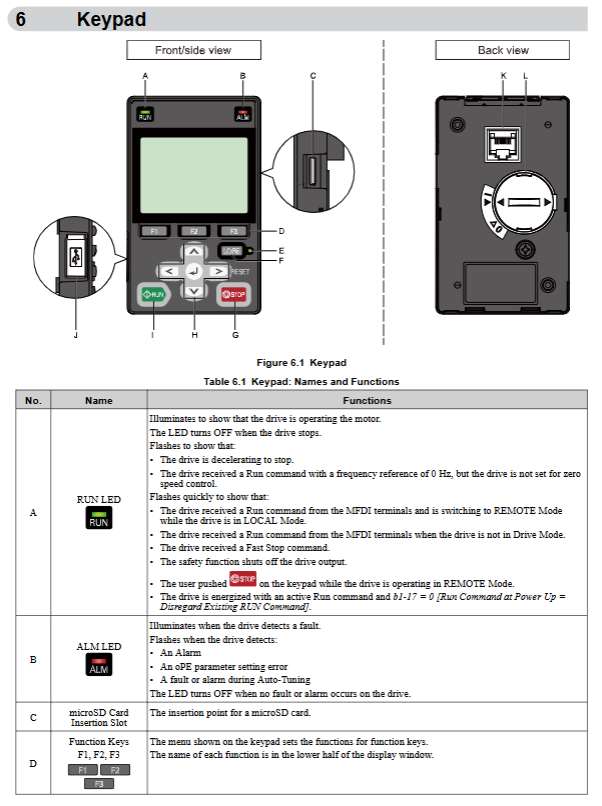
Operator functions: including data display area, ESC key, RESET key, RUN key, up and down arrow keys, STOP key, ENTER key, LO/RE switch key, which can realize mode switching, parameter editing, operation monitoring, fault reset and other operations.
Display and indicator lights: RUN indicator light displays the running status, LO/RE indicator light displays the local/remote mode, ALM indicator light displays the fault status, and frequency, current, parameter and other information can be viewed through the digital display area.
Core Programming Settings
Control mode selection: Set through parameter A1-02, supporting V/f control (0), open-loop vector control (2), and open-loop vector control of permanent magnet synchronous motor (5).
Application preset parameters: Select 7 types of application presets (pumps, conveyors, etc.) through parameter A1-06, automatically configure the optimal parameters, and simplify debugging.
Basic parameter configuration: including acceleration/deceleration time (C1-01~C1-11), carrier frequency (C6-02, 2-15kHz optional), motor parameters (E2-01~E2-12, configurable through automatic adjustment function), frequency command source (b1-01), etc.
Start up process
Initialization settings: Select control mode and application presets based on the application scenario, and initialize parameters (A1-03).
Auto Ajuste: divided into rotary type (motor rotation, adapted to open-loop vector control) and stationary type (motor non rotation, adapted to V/f control), used for automatically configuring motor parameters to ensure control accuracy.
Trial operation: No load test (to confirm motor steering, acceleration/deceleration stability) → Load test (to verify operating status and parameter effectiveness) → Jogging operation (FJOG/RJOG function, 6Hz low-speed test).
Troubleshooting
Fault classification and warning
Fault types: including hardware faults such as overcurrent (oC), overvoltage (ov), overload (oL1/oL2), overheating (oH), operational errors such as communication errors (CE), parameter errors (oPE), and adjustment errors during the Auto Ajuste process.
Warning method: When a fault occurs, the LED operator displays a fault code and the ALM indicator light remains on; The ALM indicator light flashes when there is a minor malfunction or alarm.
Common troubleshooting solutions
Overvoltage (ov): Extend deceleration time (C1-02, etc.), install braking resistors, enable overvoltage suppression function (L3-11=1), check input voltage spikes.
Overcurrent (oC): Check motor insulation and wiring, reduce load, extend acceleration time, lower carrier frequency, confirm motor type matches control mode.
Overload (oL1): Reduce load, extend acceleration/deceleration time, check motor rated current configuration (E2-01), confirm motor cooling system is normal.
Parameter Error (oPE): Verify the parameter configuration logic (such as matching carrier frequency and cable length), restore default parameters, and reconfigure.
Fault reset method
Manual reset: Reset by pressing the RESET button on the operator.
Automatic reset: Configure parameter L5-01 to set the number of automatic retries.
Power off reset: Disconnect the power supply for ≥ 5 minutes and then power it back on (applicable to serious faults).
Regular inspection: Check cable aging, cooling fan operation status, capacitor and IGBT status every 6 months to 1 year (monitored through U4-05/U4-07).
Maintenance cycle: When the service life of the cooling fan expires (U4-04 ≥ 90%), it needs to be replaced in a timely manner; Replace capacitors and IGBTs when they reach the maintenance threshold.
Maintenance of key components
Cooling fan: Regularly clean the dust on the fan blades, replace them when damaged or aged, and reset the parameter o4-03=0 after replacement.
Terminals and cables: Check the tightness of the wiring to avoid looseness and overheating; Replace aging cables in a timely manner to ensure insulation performance.
Inverter replacement: During replacement, parameter configuration can be transferred through a detachable terminal block to reduce the workload of reprogramming.
Peripheral Devices and Options
Peripheral Device Adaptation
Protective equipment: Molded Case Circuit Breakers (MCCBs), Residual Current Circuit Breakers, Thermal Relays (OL), etc. must be installed to comply with local electrical regulations.
Filtering and reactors: Input filters, EMC filters, and AC/DC reactors can be installed to reduce electromagnetic interference and improve input current waveforms.
Communication Options
Supports MEMOBU/Modbus communication protocols and can be adapted to more bus protocols by extending the communication card. Wiring must follow communication specifications and configure corresponding parameters (such as baud rate and address).
Technical Specifications and Parameter List
Core specifications
Output characteristics: Voltage range 0- input voltage, frequency range 0-400Hz, overload capacity of normal working mode 120%/60s, overload mode 150%/60s.
Protection function: including multiple protections such as overcurrent, overvoltage, overload, overheating, phase loss, and ground fault.
Parameter List
Parameter grouping: divided into initialization parameters (A), application parameters (b), adjustment parameters (C), motor parameters (E), terminal function parameters (H), protection function parameters (L), monitoring parameters (U), etc., covering all configurable items such as control mode, operating parameters, protection thresholds, etc. Each parameter is labeled with default values, configuration ranges, and functional descriptions.
Key technical points
Motor adaptation
Supports ordinary induction motors and permanent magnet synchronous motors (PM). Permanent magnet synchronous motors require motor code (E5-01) and related parameters (E5-02~E5-24) to be configured, and speed search function (b3-01=1) to be enabled.
Motor parameter configuration: Accurate input of motor rated current, number of poles, rated power, and other information is required, or automatically obtained through the Auto Ajuste function to ensure control accuracy.
Differences in Control Modes
V/f control: Suitable for ordinary speed regulation scenarios (such as fans and pumps), with a simple structure and support for multi motor control.
Open loop vector control: suitable for high-precision speed regulation and high starting torque scenarios (such as conveyors and cranes), requiring Auto Ajuste to optimize parameters.
Permanent magnet synchronous motor control: efficient and energy-saving, suitable for scenarios with variable torque and high energy efficiency requirements, requiring dedicated parameter configuration.
Core taboos for safe operation
Prohibited items: live wiring/plugging of components, use of single-phase motors, covering of heat dissipation ports, modification of internal circuits of frequency converters, use of mismatched voltage power supplies.
Required items: reliable grounding, operation after power outage and discharge, operation by qualified personnel, tightening terminals according to specifications, regular maintenance of cooling system.
The user manual for YASKAWA 120 series I/O modules (compatible with MEMOCON GL120, GL130 PLC) covers the specifications, installation wiring, I/O allocation, MEMOSOFT operation and maintenance of three types of modules: digital I/O, analog I/O, and register I/O. It specifies the voltage range of the module (such as digital input 100/200VAC, 12/24VDC, analog output ± 10V/4-20mA), point configuration (16/32/64 points, etc.), wiring specifications, I/O address allocation rules, and safety operation requirements (such as grounding resistance ≤ 100 Ω, hot plug support), and is responsible for module installation, debugging, and maintenance.
Module classification and core specifications
Module category subdivision type Key parameters Typical models
Digital input module 100VAC 16 point rated voltage 100VAC, input current 7mA, input delay ≤ 35ms JAMCS-120DAI54300
200VAC 16 point rated voltage 200VAC, input impedance 28.6k Ω (50Hz) JAMCS-120DAI74300
12/24VDC 64 point rated voltage 12/24VDC, input current 2/4mA, supports hot swappable JAMCS-120DDI36400
Digital output module 12/24VDC 32 point (current injection) load current 0.3A/point, total load 0.4A/4-point JAMCS-120DDO35410
Relay 16 points support AC200V/DC24V, contact life ≥ 100000 times JAMCS-120DRA84300
Configuration requirements: Supports MEMOSOFT version ≥ 1.21 (DOS) for 64 point modules, corresponding CPU version (such as CPU 10 ≥ 00A01)
Core operations: Module type setting (input the last 11 digits of the model), I/O address starting value configuration, data format (BIN/BCD), bit sequence (MSB/LSB)
Special settings: Simulation module software filtering (no filtering/3-time average/5-time average), register module read/write cycle (8CH minimum 32ms)
Maintenance and troubleshooting
Maintenance points
Fuse replacement: Authorized personnel only, specifications match (such as DC8 point module 3.5A fuse)
Insulation testing: Regularly use a 500VDC megohmmeter to test, with insulation resistance ≥ 100M Ω
Battery maintenance: The lithium battery (3.6V) of the register module has a lifespan of about 10 years and needs to be replaced if the voltage is ≤ 2.8V
Common Faults
Over range: ERR indicator light is on, check the input/output signal range (such as analog input ± 10V exceeding ± 10.24V)
Power supply abnormality: The P.OK light is not on. Check the polarity and voltage range of the ± 12V/+5V power supply
Communication failure: The ACTION light is not on. Please verify that the I/O allocation matches the module model
Core function: Pulse counting (supports carry/borrow), outputs coincidence signals by comparing the current value with the preset value
Coincidence mode: 3 types (current value>preset value, current value=preset value, current value<preset value)
Key features: After power on/reset, the current value is reset to zero from the preset value, and the coincidence signal can be reset when the output is disabled
(2) Cyclic counter
Core function: Automatically reset to zero when the current value reaches the preset value or counting width, loop counting
Default parameters: The preset value and counting width are automatically set to 100 after power on
Key feature: When the counting width is set to 0, the counter stays at 0 and does not perform addition or subtraction counting
(3) Sampling counter
Core function: When receiving external sampling signals, latch the current value and store it in the input register
Sampling requirements: Sampling period ≥ 10ms, pulse width ≥ 5ms
Storage allocation: Counter 1 data is stored in input registers 1-2, counter 2 is stored in registers 3-4
(4) Storage counter
Core function: Latch the current value when triggered by external sampling signals, store up to 999 sets of data, and support reading from specified addresses
Key feature: Output coincidence signal when storage reaches preset value, clear storage data when output is disabled
Reading method: Specify the address through pointer commands, and only read stored data when the command is ON
Environmental restrictions: Prohibit direct sunlight, condensation, corrosive gases, and severe vibration environments
Installation operation: The tightening torque of the module fixing screws meets the standard, and the unused slots need to be covered with dust covers
Switch setting: SW1 is used to switch the number of counting bits (OFF=6 bits, ON=8 bits), SW2 is not used
(2) Wiring requirements
Cable selection: Shielded twisted pair cable is used for signal lines, with a length of ≤ 30m (when 50kpps)
Anti interference measures: The distance from the power line is ≥ 30cm, the shielding layer is grounded at a single point, and a filter is installed on the external power supply
Terminal wiring: Signals such as pulse input, external sampling, and counting enable should be wired according to the terminal definition to avoid misconnection
Test run and troubleshooting
(1) Test running process
Before powering on, check the correctness of switch settings, terminal wiring, and voltage levels
Power on self-test: If the RDY indicator light is on, it indicates that the module is normal (self-test for about 0.8 seconds)
Function verification: Operate the pulse generator and observe the status of PHA/PHB (pulse input) and INC/DEC (counting direction) indicator lights
(2) Common troubleshooting
Common causes and solutions for fault phenomena
Non count count enable not activated, pulse input mode error, wiring error check output coil “count enable” status, pulse mode in initial settings, terminal wiring
Coincidentally, the preset value for abnormal output is set incorrectly, the output is disabled but not turned off. Check the preset value parameters and ensure that the output disabled coil is turned off
RDY light goes out, ROM/RAM error, WDT timeout module reset or power off restart, if ineffective, replace the module
Safety regulations
Operation safety: Wiring and maintenance must be powered off, touching live terminals is prohibited to avoid electric shock
Personnel requirements: Installation and wiring must be carried out by professionals to avoid wiring errors that may cause fires or equipment damage
Prohibition of modification: It is not allowed to disassemble or modify modules. Modified products are not covered by warranty and may pose safety risks