Call us 24/7uaedcs@163.com
Welcome to the official website of CNIACS Automation Technology Co., Ltd!
Call us 24/7uaedcs@163.com

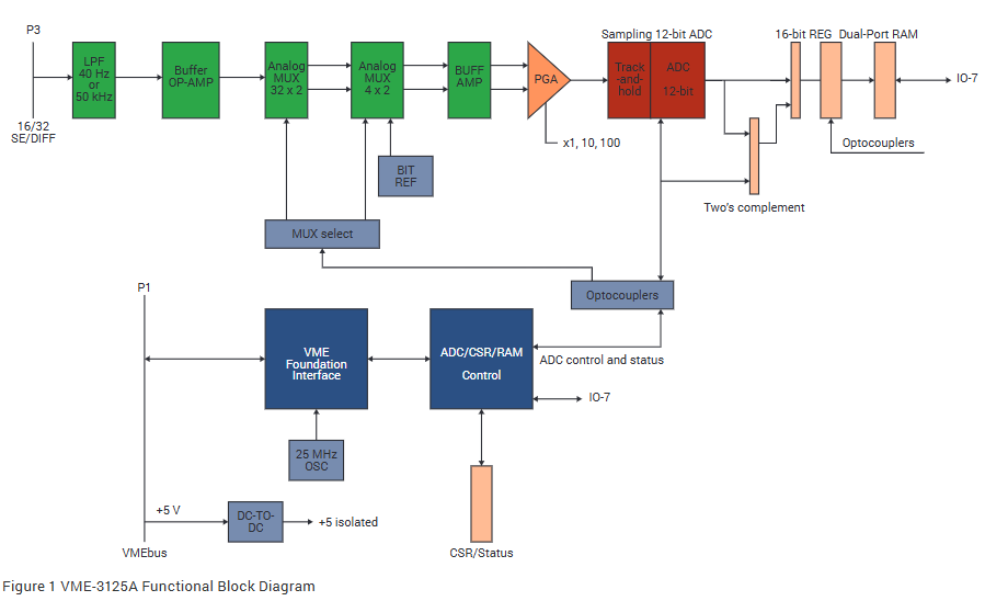
GE VMIACC-5595 2 Gb/s Reflective Memory Hub Component

Basic Information

Product Name: VMIAC-5595 2 Gb/s Reflective Memory Hub Component

Production company: GE Fanuc Automation (Embedded Systems Division)

Document information: Published on May 16, 2007, document number 800-805595-000 E. Specifications may change without prior notice

Main features

VMIxxx-5565 Reflective Memory Network Product for GE Fanuc Embedded Systems

Use small form factor pluggable (SFP) transceivers, providing up to 8 ports

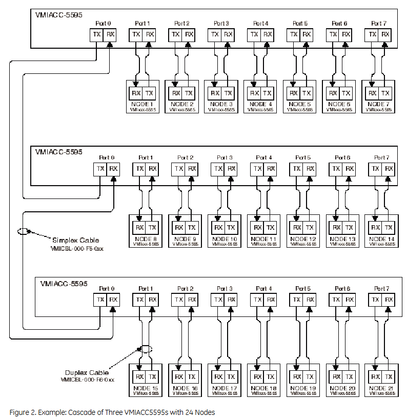
Hub components can be cascaded and support up to 256 nodes

Automatically bypass defective or disconnected nodes in fiber optic networks

The automatic bypass function can be controlled by signal loss or synchronization mode loss

Regenerate serial optical signals at each port, eliminate link loss and reduce jitter

Can be configured to use cables up to 10km in length

10BaseT Ethernet TCP/IP port for remote access and control

RS232 port is used for local access and control

Optional 19 inch 1U rack installation or desktop enclosure

Built in universal power supply

Dark to Dark “option: If the receiver does not detect a signal, the onboard transmitter can be turned off (applicable to firmware version 02.00 and higher)
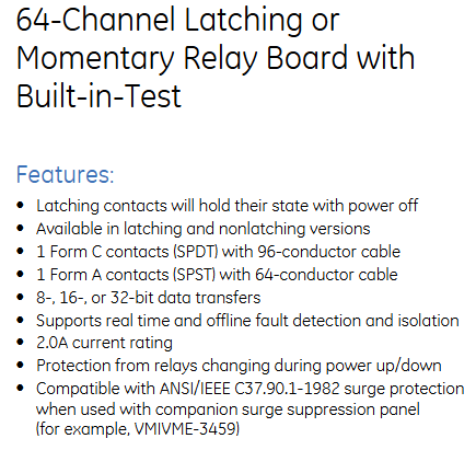
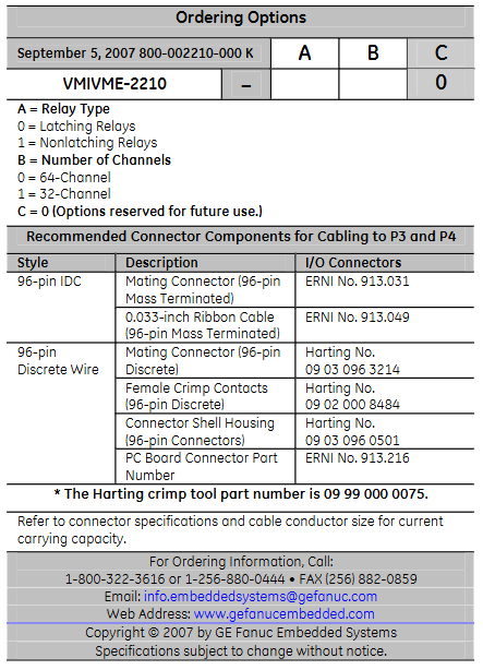
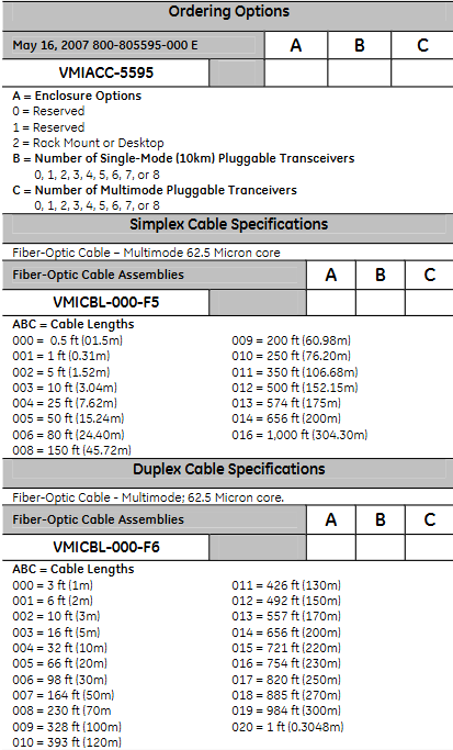
Ordering Options

Option Description

A (shell option) 0=reserved; 1=Reserved; 2=Rack installation or desktop

B (number of single mode (10km) pluggable transceivers) 0, 1, 2, 3, 4, 5, 6, 7 or 8

C (number of multi-mode pluggable transceivers) 0, 1, 2, 3, 4, 5, 6, 7, or 8

Cable specifications

1. Simplex cable specifications

Fiber optic cable – multimode 62.5 micron core

Fiber optic cable assembly: VMICBL-000-F5, cable length code ABC corresponds to different lengths, such as 000=0.5 feet (0.15m), 001=1 foot (0.31m), etc

2. Duplex cable specifications

Fiber optic cable – multimode; 62.5 micron core

Fiber optic cable assembly: VMICBL-000-F6, cable length code ABC corresponds to different lengths, such as 000=3 feet (1m), 001=6 feet (2m), etc

Functional characteristics

1. Port wavelength and distance

Multimode port wavelength: 830 to 860nm, multimode cable length: maximum 300m

Single mode (10km) port wavelength: 1300 to 1335nm, single mode (10km) cable length: maximum 10km

Single mode (80km) port wavelength: 1540 to 1570nm, single mode (10km) cable length: maximum 80km

2. Core functions

It is a hosted hub designed to be used in conjunction with GE Fanuc’s VMIxxx-5565 series reflective memory real-time network products for embedded systems

When signal loss or loss of effective synchronization mode is detected, the port can be automatically bypassed to keep other nodes in the network running

The optical port adopts a small form factor pluggable (SFP) transceiver, which only needs to be configured with the required port. It can be combined with multi-mode (short distance) or single-mode (long distance) transceivers to save small network costs and optimize the system

For large networks, multiple VMIAC-5595 components can be cascaded, supporting up to 256 nodes

The reflective memory network can be monitored and controlled through a simple PC serial port (RS232 port) or through a local area network (LAN) or web browser (Ethernet port)

3. Control and Status

Additional control registers allow manual disabling of transmitters on any port

The front panel manual switch includes a received momentary reset switch and a Gang Select switch. The Gang Select switch configures the VMIACC-5595 port as an 8-port loop or two independent 4-port loops

The three LEDs next to each port provide visual indications of port status, and additional status indications and operating modes can be obtained through serial or Ethernet ports

The status information includes detection of installed transceivers, detection of signals (light), detection of effective synchronization modes, and port operation speed (2Gb/s)

Control registers allow channel bypassing based on the absence of a single valid synchronization mode or multiple synchronization modes, as well as signal (light) loss. Each port can be manually activated or bypassed, regardless of the status indicator

4. Ethernet controller

10BaseT interface conforms to Transmission Control Protocol/Internet Protocol (TCP/IP) standard

Each hub component has a unique MAC address and can run on a local area network (LAN) or a wide area network (WAN)

Contains a remote user interface available via standard Ethernet connection, controlled by a standard HTML based web browser, displaying status data, supporting bypass mode, “dark to dark”, and forcing each port on/off or automatic, all of which are saved in NVRAM

Physical/Environmental Specifications

1. Size

Desktop component size: 16.73 inches wide x 10.0 inches deep x (1U) 1.72 inches high (excluding non slip self-adhesive feet)

Rack mounting component size: Same as the basic size of desktop components, but includes two 1U rack mounting brackets for standard 19 inch racks

2. Connectors

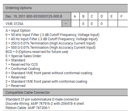
Front panel connectors: 8 industry standard SFP transceivers, SFP sockets without transceivers include EMI dust plugs, 1 RJ45 Ethernet connector, and 1 9-pin female D-subminiature RS232 connector

Rear panel connector: includes power input module, including power on/off switch, 4A/250V fuse, and globally compatible IEC socket

3. Wiring

Each installed SFP transceiver requires one duplex LC fiber optic cable or two simplex LC fiber optic cables. Simplex cables are best suited for cascading hubs, while duplex cables can be used for all other interconnections

4. Power requirements

90 to 264VAC, 47 to 440Hz, 25W

The power supply and power input module comply with safety standards: UL, C-UL: UL 1950; TUV:EN69050; CE:EN55022、EN61000-4-2、3、4、5; EN61000-3-2

Fuse: 1A, 250V, 5 × 20mm, fast acting, IEC 60127-2 standard glass or equivalent product

5. Environmental parameters

Temperature: Operating temperature from 0 ° C to+65 ° C; Storage temperature from -40 ° C to+85 ° C

Humidity: Operating relative humidity of 20% to 80%, no condensation; Storage relative humidity of 20% to 80%, no condensation

MTBF: total fit x quantity: 2317.3641; MTBF (hour): 431524.76

6. Regulatory certification

EU (CE mark): Complies with multiple standards such as EN55024, EN55022 Radiation Emission Class A, etc

United States: FCC Part 15, Class A

Canada: ICES-003, Grade A

Safety: Designed to comply with safety standards such as UL60950 and EN60950 (LVD)

GE VME-3125A Isolation Scan 12 Bit 32 Channel Analog

Basic Information

Product Name: VME-3125A Isolation Scan 12 Bit 32 Channel Analog to Digital Converter Board (with Built in Testing Function)

Production company: Abaco Systems

Main features

32 single ended or 16 differential inputs

Automatic scanning, continuously digitizing input and storing results in dual port data registers

Input range: Bipolar ± 50mV to ± 10V, Monopolar 0-100mV to 0-10V, or 0 to 25mA current input options

Jumper programmable gains x1, x10, x100

1 12 bit A/D converter with built-in tracking and holding functions

Start scanning without software startup

Pause and lock scanning function, which can achieve 40KSPS arbitrary channel sampling based on channel pointer

Optional A/D range: ± 5V, ± 10V, 0 to+10V

40kHz total conversion rate

Support real-time built-in testing (BIT)

Input connector compatible with discrete and ribbon cables

Optional data encoding: offset binary or binary complement

Over voltage protect

Low pass input filter: 50kHz, optional 40Hz

Pull down resistor to prevent input floating

1000V analog ground/digital ground isolator

Ordering Options

Option Description

A (input option) 0=50kHz input filter (-3dB cut-off frequency, voltage input); 1=40Hz input filter (-3dB cut-off frequency, voltage input); 2=250 Ω 0.01% terminal (high-precision current input); 3=500 Ω 0.01% terminal (high-precision current input)

BCD 0 (reserved for future options)

E (Special Sales Order) 0=Standard; 1=Reserved for CCS

F (conforming coating) 0=standard VME front panel without conforming coating; 1=Reserved; 2=Standard VME front panel with conforming coating; 3=Reserved

Compatible cable connectors

Standard 37 pin ultra small D-type male connector

Discrete cabling: AMP 747916-2 (with 206478-4 enclosure)

Ribbon cable: AMP 747306-1

Functional characteristics

1. Basic Introduction

VME-3125A provides isolated 12 bit analog-to-digital conversion with 32 single ended analog voltage input channels (16 differential) for VMEbus’s 6U Eurocard. The optional gain and A/D range support an input voltage range of ± 50mV to ± 10V, and the current input option supports 32 single ended channels with ranges of 0 to 20mA, 4 to 20mA, and 5 to 25mA. To minimize system software overhead, all inputs are continuously scanned and digitized at a total sampling rate of 40000 samples per second, and the measurement data of each channel is accessed by VMEbus at any time through a dual port data register. For voltage input, a 40Hz low-pass input filter can be selected to minimize the impact of system noise, and the standard unit is equipped with a 50kHz low-pass filter.

2. Core functions

Programmable Gain Amplifier (PGA): Jumper options include series voltage gain x1, x10, or x100 for all channels; For voltage input, the full range of the A/D converter can be selected as ± 5V, ± 10V, or 0 to+10V; the data encoding software can be selected as offset binary or binary complement code

Input configuration: The input can be configured with 16 differential voltage channels or 32 single ended voltage or current channels through jumper wires; A single front panel 37 pin ultra small D-type connector provides connections for all input channels

Working mode: All 16 or 32 input channels are continuously scanned at the maximum sampling rate, and the resulting data is stored in a dual port data register for VMEbus to access; After any reset operation, the scan automatically starts without the need for additional programming to initiate the A/D conversion process

Built in Test Function (BIT): By selecting the BIT working mode, the operation of PGA, ADC, and related control logic can be verified. In this mode, the internal reference voltage is applied to the input of PGA, bypassing the analog input multiplexer. All data channels read through the control interface will reflect the selected BIT reference voltage

3. Features related to VMEbus

Compliance: Compliant with VMEbus standard ANSI/IEEE STD 1014-1987, IEC 821 and 297, with 6U external dimensions

Board address: The physical address is selected through the onboard address jumper, using VMEbus address lines A07 to A15; The VME-3125A board occupies 128 bytes of address space and can be located on any 64 word boundary of the short I/O (A16) space

Address Modifier: Address modifier bits are selected and decoded through jumpers to respond to non privileged short I/O access, monitoring short I/O access, or both access privileges

4. System reset and indicator lights

System reset: System reset establishes the following board states: all channels automatically scan, front panel diagnostic LED indicator lights up, offset binary data format

Front panel system diagnostic LED: The software controlled front panel LED lights up when the system is reset and can be turned off under software control to provide an external indication that the built-in test has been completed

Simulate input data format

The analog input is digitized and stored in 32 dual port data registers (16 registers for differential operation) as a 12 bit right aligned digital value. The software can select data codes as offset binary and binary complement. In binary complement encoding, the sign bit (D11) is extended to the most significant bit (D12 to D15) of the data register.

Input characteristics

(At+25 ° C and rated power supply, unless otherwise specified)

Number of channels: 32 single ended or 16 differential voltage input channels; 32 single ended current input channels

Voltage range: ± 50mV to ± 10V (bipolar) or 0 to+100mV, 0 to+10V (unipolar), factory configured for ± 10V input range

Current terminal: Suitable for single ended, 0-10V, and X1 gain unipolar configurations, with two options: 250 Ω 0.01% and 500 Ω 0.01%

Current range: According to the applicable input range of the terminal, 250 Ω corresponds to 0 to 20mA, 4 to 20mA, 5 to 25mA; 500 Ω corresponds to 0 to 20mA, 4 to 20mA

Input impedance: When the power is turned on, the voltage input options are DC differential 27M Ω, DC common mode 1.3M Ω, AC differential 9K Ω, and AC common mode 9K Ω. When the power is turned off, the DC differential 11K Ω, DC common mode 6K Ω, AC differential 9K Ω, and AC common mode 5K Ω

Input bias current: minimum 44nA/maximum 90nA

Input bias current drift: 0.30nA/° C

Common mode voltage (CMV): When the differential input is at zero input signal, the maximum ± 11V; CMV refers to the common analog ground of all inputs; For other gains, the formula is ± 11V=(VCM+Vddiff/2) * gain

Common mode rejection ratio (CMRR): Differential input has different minimum/typical values (dB) at different gains and ADC ranges when the source is unbalanced at 350 Ω and the frequency is between DC and 60Hz

Input to VMEbus isolation: 1000VDC

Input noise: Under 10 to 1000Hz and 3 σ, different gains and ranges have different maximum noise (mV p-p) in single ended mode

Each input bandwidth: DC to Fc, where Fc is 50kHz for a 50kHz filter and 40Hz for a 40Hz filter option unit

Input filter: Single pole passive low-pass filter, -3dB at 50kHz or 40Hz ± 20% (voltage input option only)

Overvoltage protection: maximum ± 40V continuous during power supply; ± 25V during power outage

Transmission characteristics

(At+25 ° C and rated power supply, unless otherwise specified)

Measurement resolution: 12 bits

Channel scanning rate: minimum 40KSPS (thousand samples/second) total rate

Voltage transfer function:

E IN=E LO+E FSR × 4096N ADC, where E IN=input voltage, E LO=lower end of input range,

E FSR=full-scale input range, N ADC=A/D converter reading

Current transfer function: I IN=R TERMINATION E FSR × N ADC/4096, where I IN=input current (ampere), E FSR=10V (unipolar), N ADC=A/D converter reading, R TERMINATION=250 Ω or 500 Ω options

Input range of A/D converter: ± 5V, ± 10V, 0 to+10V, jumper optional

Input gain of A/D converter: x1, x10, x100 (± 0.3%, jumper optional)

Accuracy: Voltage input=± 0.04% reading ± 0.03% range ± 2.0mV; Current input (-200, -300 options)=± 0.05% range ± 2.44 μ A

Temperature stability: The voltage input board option (mV/° C) is ± 30PPM reading ± 25PPM range ± 20 μ V; The current input board option (μ A/° C) is ± 40PPM reading ± 25PPM range ± 20nA

Long term drift: ± 50PPM reading ± 45PPM range ± 100 μ V every 1000 hours

Channel crosstalk: In ± 10V bipolar and gain X1 differential mode, different options have different typical/maximum values (dB) for DC and AC inputs

BIT reference voltage: Software options include 0.000V,+4.980V,+0.4928V, and 9.91mV

BIT reference accuracy: ± 30mV ± 30PPM/° C (4.98VDC)

Physical/Environmental Specifications

Size: Standard VME double height board 160 × 233.5mm

Power requirement:+5VDC (± 5%), maximum 1.5A

Temperature: Operating temperature from 0 ° C to+65 ° C; Storage temperature from -40 ° C to+85 ° C

Humidity: Operating relative humidity of 20% to 80%, no condensation

Cooling: forced air convection (standard VME slot)

MTBF: Contact the factory

Input connector (P3): 37 pin ultra small D-type female connector

GE VME-3122A High Performance 16 Bit Analog

Basic Information

Product Name: VME-3122A High Performance 16 Bit Analog to Digital Converter (ADC) Board

Production company: GE Fanuc Intelligent Platforms

Main features

64 different or single ended inputs

16 bit analog-to-digital (A/D) conversion

Software selectable conversion rate (maximum 100kHz)

Programmable options for scanning channels 1, 8, 16, 32, or 64

Continuously digitize the selected input channel and store the results

Three triggering modes: software triggering, external triggering, and interval timer triggering

Three scanning modes: automatic scanning, single scan, and random access

Programmable VME interrupt

User programmable interval timer

Software programmable gains 1 and 10

External triggering can synchronize multiple boards simultaneously

Jumper selectable A/D range: 0 to+5V, 0 to+10V, ± 2.5V, ± 5V, and ± 10V

Optional low-pass filter

Over voltage protect

1024 word data buffer (16 word deep buffer x 64 channels)

Optional output encoding

When powered on, it is in automatic scanning mode with a gain of 1

Application Fields

Factory automation and instrumentation

process control

laboratory instruments

Machine monitoring

data acquisition

Ordering Options

Option Description

A (input filter option) 0=no filter; 1=10Hz(-3dB); 2=50Hz(-3dB); 3=100Hz(-3dB); 4=500Hz(-3dB)

B (channel quantity option) 0=64 channels high performance; 1=32 channels high performance; 2=16 channels high performance

C (input option) 0=differential analog input channel with 96 pin non latch connector; 1=Single ended analog input channel with 96 pin non latch connector; 2=Differential analog input channel with 64 pin latch connector; 3=Single ended analog input channel with 64 pin latch connector

DE 0 (reserved for future options)

F (Special Sales Order) 0=Standard VME front panel without conforming coating; 1=Reserved; 2=Standard VME front panel with conforming coating

Connector data

Recommended style for connecting components P3 and P4 I/O connectors

64 pin IDC mating connector (64 pin) Panduit 120-964-435

Strain relief (applicable to 64 pin connectors) Panduit 100-000-072

96 pin discrete mating connector (96 pin discrete) AMP 925486-1

Female crimping contact (96 pin discrete) AMP 530151-6

Connector housing (suitable for 96 pin connectors) Harting 09 03 096 0501

96 pin IDC mating connector (96 pin large-scale termination) ERNI 913.031

0.033-inch ribbon cable (96 pin large-scale termination) ERNI 913.049

Strain relief insert (0.033-inch ribbon cable) Harting 09 02 000 9912

Connector housing (suitable for 96 pin connectors) Harting 09 03 096 0501

PC board I/O connector part number Panduit 101-096-033A

Functional characteristics

1. Working mode

MODE

Software trigger: Start the selected scanning mode by writing the software trigger address

External trigger: The external trigger received on the P2 connector initiates the selected scanning mode

Interval timer trigger: Start the selected scanning mode each time the programmed time interval expires

SCAN

Automatic scanning: default scanning mode, all active channels are scanned continuously in order

Single scan: Start a single data burst (scanning all selected channels) from the selected trigger mode, stop and wait for another trigger after scanning all selected channels

Random access: Each time the selected trigger mode is enabled, a single channel can be selected, digitized, and stored

Channel automatic gain: The unique gain code for each channel is loaded from VME into the gain buffer, and the allocated code is retrieved in real-time from the buffer during each channel acquisition

Synchronization: A single scan or burst can be initiated by an external TTL trigger through the P2 connector (external trigger) or a local trigger through the control and status register (CSR) (software trigger), and any event will generate a P2 trigger output, which can be used to synchronize up to 15 cards

2. VME related characteristics

VME access: The response to the address modifier can be selected as A32, A24, or A16 address space through jumper wires; Monitoring or user privileges, or both

VMEbus compliance: Compliant with VMEbus specifications ANSI/IEEE STD 1014-1987, IEC 821 and 297, with 6U external dimensions

VME interrupt: An interrupt request can be generated at the end or in the middle of a buffer scan, or it can be initiated after collecting a specific number of samples (1 to 65535), and the response vector is controlled through the interrupt vector register

Data ready flag: When the data buffer is full (end of scan) or half full (middle of scan), the data ready flag in CSR is set

Interval timer: Programmable interval timer provides a time interval of up to 687 seconds

3. Reset operation

Board reset response system reset or writing software reset address

The reset operation automatically establishes the following default conditions: automatic scanning mode, 64 channel block size, 64 channel data buffer, channel gain=x1, 100kHz conversion rate

ADC will undergo a calibration cycle under any reset condition, which takes 41ms after the reset operation is initiated

4. Other functions

PGA: Channel gains of x1 and x10 can be selected through a programmable gain amplifier (PGA). The PGA gain can be configured through software as a single gain for all channels, or real-time control can be used to assign unique gains to each channel

Panel indicator: The front panel LED controlled by the program is powered on during the reset period and turned off through CSR

Board Identification: The Board Identification Register (BIR) contains the VME-3122A identification code

Input characteristics

Number of input channels: 64, 32, or 16 differential or single ended channels

Full range A/D range: ± 2.5V, ± 5V, ± 10V, 0 to+5V, 0 to+10V, jumper optional

Channel gain: Software configuration is x1 or x10

Full range input range

Gain=1: ± 2.5V to ± 10V (bipolar); 0 to+5V, 0 to+10V (unipolar)

Gain=10: ± 250mV to ± 1V (bipolar); 0 to+0.5V, 0 to 1V (unipolar)

Accuracy (% of FSR): There are different values for different ranges and gains, based on the average of 1000 samples

Stability: Temperature drift, per degree Celsius=± 25PPM (ADC reading) plus ± 5PPM (ADC range) plus ± 2.5 µ V

Input noise: (0.4+0.3/G) mV, where G=PGA gain (noise is independent of filter options)

Input bias current (typical/maximum): 50/120nA

Input impedance (minimum): Different DC differential, DC common mode, AC differential, and AC common mode impedances when the power is turned on and off

Channel crosstalk (DC to 1kHz): 80dB between adjacent channels within ± 10V range; 70dB between adjacent channels within ± 2.5V range

Common mode voltage range: (IVCM |+| VIN |. G) ≤ 10V, where VCM=common mode voltage, VIN=input voltage, G=gain

Common mode rejection: From DC to 60Hz, when the 350 Ω source is unbalanced, the minimum common mode rejection for gain 1 is 68dB, typical 80dB; the minimum common mode rejection for gain 10 is 76dB, typical 89dB; the minimum common mode rejection for+5V and ± 2.5V ranges is 66dB, which can be adjusted on-site to achieve the same common mode rejection as gain 1

Overvoltage protection: ± 35V (continuous) power on/off; ± 80V (transient, maximum 1s)

Input filter: Optional low-pass single pole filter with different -3dB values at different frequencies, frequency doubling in single ended (pseudo differential) applications, cut-off frequency tolerance of ± 25%, unfiltered input bandwidth (20Vp-p) typically 40kHz

Common mode/floating input protection: Both sides of each input are grounded through a 22M Ω resistor

Transmission characteristics

Resolution: 16 bits

Input sampling: order, starting from channel 00

Input transfer function:

E IN=E LO+E FSR × 65536N ADC, where E IN=input voltage, E LO=lower end of input range, E FSR=full-scale input range, N ADC=A/D converter reading

A/D conversion rate: 381 to 100kSPS

Channel sampling rate (maximum): 100kSPS (100kSPS ÷ number of channels in the scan block, minimum 1 channel)

Time interval: 305 µ s to 687s

Data encoding: programmable to choose binary complement or direct/offset binary

Data buffer storage

Buffer size: 16 to 1024 consecutive 16 bit data words, program controlled

Block size: 1, 8, 16, 32 or 64 channels, program controlled

Access time: maximum 600ns during non scanning; typical 600ns during scanning, maximum 1.2 µ s (maximum access time in scanning mode only occurs when VME access occurs within the ADC sampling window)

VME access: D8 to or D16

Availability: Can be accessed from VME at any time, buffer and block sizes are controlled through configuration control registers (CCR)

Physical/Environmental Specifications

Size: 6U (4HP) single slot Eurocard shape

Height: 9.2 inches (233.4mm)

Depth: 6.3 inches (160mm)

Thickness: 0.8 inches (20.3mm)

Power requirement: 3.0A at+5VDC (maximum)

Airflow: Forced air cooling is required

Temperature: Operating temperature 0 to+65 ° C; Storage temperature -40 to+85 ° C

Altitude: Working at 0-10000 feet (3000m); Storage 0-40000 feet (12000m)

Humidity: Working relative humidity 0% to 80%, no condensation

Input connectors (P3, P4): can be ordered as 96 pin DIN non latch or 64 pin DIN latch. The center row of the 96 pin non latch connector is grounded, while the center row of the 64 pin latch connector is not grounded. When using the 64 pin latch connector in differential mode, users can provide grounding on the front panel jumpers E1 and E2, which will result in channels 31 and 63 being configured as single ended

UIOC support

In UIOC, VME-3122A is used as a monitoring device. During initialization, UIOC programs VME-3122A to scan all 64 channels and sets the scanning mode to automatic scanning. Through UCLIO ™ Language, users can set programmable channel gains and command UIOC to retrieve data from any or all channels of VME-3122A. Through a menu driven calibration process, users can create and store channel gain and offset correction factors, which UIOC automatically uses to provide software gain and offset correction for each channel.

GE VMIVME-2536 32 channel optically coupled digital I/O board 

Basic Information

Product Name: VMIVME-2536 32 Channel Optical Coupled Digital I/O Board (with Built in Testing Function)

Production company: GE Fanuc Automation (Embedded Systems Division)

Core function: Includes 32 optically coupled inputs and 32 optically coupled outputs, both with built-in testing (BIT) capability, providing continuous 1kV system isolation for VME backboards

Main features

32 optically coupled outputs and 32 optically coupled inputs

High isolation potential: continuous 1kV, pulse 35kV

Supports 8-bit, 16 bit, and 32-bit data transmission

Supports A24 standard data or A16 short I/O addressing

Input can be subjected to voltage induction or contact induction

The input voltage range is 5 to 125VDC

Output current up to 300mA, maximum output voltage 50V

Built in testing that supports input and output

Ordering Options

A (input voltage range): 0=5V, 1=12V, 2=24-28V, 3=48V, 4=125V (voltage induction only), 5=reserved

B: 0 (reserved for future options)

C (CE Compliance): 0=Non CE Compliance, 1=CE Compliance

DEF: 0 (reserved for future options)

Functional characteristics

1. Compliance

Compliant with VMEbus specifications ANSI/IEEE STD 1014-1987, IEC 821, and 297

Supported Address Modifiers: 3D, 39/2D, 29

Supports A24/A16 addressing, data transmission supports D32/D16/D08 (EO)

2. Built in testing (BIT)

Input testing: By setting bits in the Control and Status Register (CSR), the input is placed in test mode. At this time, the data read through the input port is from the onboard test register rather than on-site data. The test register has the same address as the input data port and supports both online and offline testing

Output testing: The contents of the output data register can be read at any time to support online testing; By setting the bit in CSR, the output can be placed in offline testing mode, where the open collector output is completely disabled. This allows for testing of data writing and reading modes in the output register without affecting the output

Power on/reset state: The board is in test mode, and the output data register should be initialized before going online to avoid uncertain states

3. Addressing scheme and address mapping

Addressing organization: Organized by 8-bit ports, including 4 input ports and 4 output ports, located on a long word boundary above the board ID and CS registers, occupying 16 bytes of address space

Address Mapping:

$00: BD ID (Board ID)

$02: Control and Status Register (CSR)

$04- $07: Input data register 0-3

$08- $0B: Output data register 0-3

$0C – $0F: Reserved

Input characteristics

Input configuration: can be set as voltage sensing or contact sensing (set according to byte boundaries); Contact sensing requires the installation of SIP resistors provided by the user; Select external voltage or internal VME+5V as contact induction mode power supply through jumper according to byte boundaries (VME+5V is only applicable to 5V input option)

Input voltage options: 5V, 12V, 24V, 28V, 48V, 125V (specific parameters are shown in Table 1-5)

Input isolation: minimum 10M Ω

Isolation voltage: 1000V continuously from the site to VME, 3500V per second; maximum continuous voltage between channels is 500V

Contact debounce: Users can program debounce with debounce times of 0, 0.256, 0.512, 1.024, 2.048, 4.096, 8.192, and 16.384ms. When resetting, debounce is set to 0 by default

Output characteristics

Output configuration: Optical isolation, open collector; Users can install pull-up resistors according to byte boundaries; Select external voltage or internal VME+5V via jumper according to byte boundaries to power the pull-up resistor

Output leakage current: maximum 500uA at VCE=50V, TA=60 ° C

Maximum output voltage: 50V

Switching time: see Table 6

Output isolation: minimum 10M Ω

Isolation voltage: 1000V continuously from the site to VME, 3500V per second; maximum continuous voltage between channels is 500V (note: user provided resistance may limit isolation)

Physical/Environmental Specifications

Size: 6U (4HP) single slot Eurocard shape

Height: 9.2 inches (233.4mm)

Depth: 6.3 inches (160mm)

Thickness: 0.8 inches (20.3mm)

User connectors: Two 64 pin DIN connectors (one for input and one for output)

Temperature: Operating temperature 0 to+60 ° C; Storage temperature -55 to+85 ° C

Humidity: 20% to 80%, no condensation

Power requirement:+5VDC, 2.65A

Mean Time Between Failures (MTBF): 463909 hours

Regulatory certification:

EU (CE mark): Complies with EN55024, EN55022 radiation emission A-level standards, etc

United States: FCC Part 15, Class A

Canada: ICES-003, Grade A

GE VMIVME-2528 128 bit TTL digital I/O TURBOModule ™

Basic Information

Product Name: VMIVME-2528 128 bit TTL Digital I/O TURBOModule ™

Document information: Document number 500-002528-000N, revised on September 30, 1994

Company Information: Produced by VME Microsystems International Corporation, with a company address of 12090 South Memorial Parkway, Huntsville, AL 35803-3308, Contact phone numbers (205) 880-0444, 1-800-322-3616

Trademark information: BITMODULE ™、 MEGAMODULE ™、 TURBOMODULE ™ The VMIC logo is a registered trademark of the company

Security Summary

Grounding requirements: To reduce the risk of electric shock, the chassis and system cabinets must be connected to electrical grounding, using a three core AC power cord and correctly grounded

Environmental restrictions: Equipment must not be operated in explosive atmospheres

Circuit safety: Operators must not remove the product casing, component replacement and internal adjustment must be carried out by qualified maintenance personnel, and components must not be replaced before power failure. Even if there is a power failure, dangerous voltage may still exist in some situations, and discharge is required before operation

Maintenance precautions: Internal repairs or adjustments must not be carried out independently, and personnel with first aid and resuscitation capabilities must be present; Do not replace components or modify the system, repairs should be returned to the company for further processing

Safety symbols: including reference manual symbols, dangerous voltage symbols, protective conductor terminal symbols, and other safety symbols and their meanings

Warning and Caution: “Warning” indicates a danger that may result in personal injury or death; CAUTION “indicates the potential danger of system damage; NOTE “indicates important information

Introduction

Product Features

128 bit TTL input/output

16 8-bit I/O port jumpers, allowing for selection of input or output operations on 8-bit boundaries

24mA current injection capability

Supports 8-bit or 16 bit data transmission

Function description: High density TTL I/O board, supports up to 128 bit TTL input or output through user installed port direction control jumpers. Each jumper sets an 8-bit port as an input or output port, and each output has a current absorption capacity of up to 24mA. It is designed with a high-quality ground plane to enhance noise resistance. When the system is reset, all I/O ports are initialized to inactive state, and all ports are activated by writing to I/O register 7

Reference materials: including “The VMEbus Specification” and various application and configuration guides provided by VMIC, such as “Digital Input Board Application Guide”

Working principle

Block diagram: The functional block diagram is divided into six sub parts: VMEbus basic logic, data transceiver, address comparison logic, read/write register control logic, registers 0-3, and registers 4-7. There are also multiple subsystem block diagrams

Board addressing: supports data transmission of monitoring or non privileged short I/O memory space, selects I/O access type through jumper, factory configured to respond to short monitoring I/O access, and has two board selection DIP switches for setting the board’s base address

VMEbus basic logic: including typical VMEbus drivers, receivers, and control logic

Register read/write control logic: Address bits A01, A02, A03 and read/write control lines are decoded into eight write control lines and eight read control lines, routed to the enable pins of each bidirectional latch, which can be selected for read or write operations through jumper wires

Data transmission description: The corresponding I/O data register is selected for data transmission through address bits A3, A2, and A1 combined with a data gating signal. The board selection signal generates an active signal for data transmission with DSO and DS1 logic gates. The board selection also activates a delay signal to generate a delayed version, which is used to provide setup time for the data transceiver during the write cycle before locking the data into the I/O register. The DTACK signal indicates that the data has been latched (write cycle) or is valid (read cycle)

I/O port enable description: The system reset signal (powered on or initiated by the VMEbus master device) disables all I/O ports/registers, and enables all I/O ports by writing to the I/O register R7L, regardless of whether they are configured as input or output ports

Programming

I/O register mapping: 12 bit addresses (A15 to A04) are used for board selection decoding, and the address switch is set to match these bits to generate data transfer board selection signals. The 128 bit I/O is divided into eight 16 bit registers for word transfer, and address bits A03, A02, and A01 are used to decode one of the eight registers, with a detailed I/O register mapping table

I/O port direction: Programming should be consistent with the I/O configuration selected by the jumper in the I/O port direction. The output port can only write data, and the input port can only read data. Please refer to Section 5 for jumper configuration details

Configuration and installation

Unpacking procedure: Product components may be sensitive to electrostatic discharge, unused boards should be stored in their original packaging, and it is recommended to use conductive materials when placing them. After receiving them, check for any transportation damage and handle them promptly

Physical installation: Power off installation or removal of the board, insert the board into the appropriate slot of the chassis, ensure correct alignment and orientation

Jumper and switch positions: Refer to Figure 5.3-1 for information on jumper and switch positions

I/O port direction jumper configuration: Table 5.4-1 specifies the use of jumpers J10 to J25, and installing jumpers will configure the corresponding ports as input ports

Address modifier: Factory configured to respond to short monitoring I/O access, installing jumper J9 can be changed to respond to short non privileged I/O access

Address selection switch: There are two address selection switches on the board, and Figure 5.6-1 shows their use in the addressing scheme

I/O cable and card edge connector configuration: The I/O connectors (P3 to P6) are 64 pin DIN standard, designed with high-quality ground planes connected to VMEbus ground and alternating I/O pins for connectors. They support connection to connectors P3, P4, P5, and P6 through four cables and have connector pin/channel allocation tables

Maintenance

Maintenance points: When the product malfunctions, it is necessary to check the software, system configuration, electrical connections, jumper or configuration options, whether the board is fully inserted, whether the connector pins are clean, whether adjacent board components are interfered with, cable and I/O connection quality, etc. If it needs to be returned for repair, it is necessary to contact VMIC to obtain a Return Merchandise Authorization (RMA) number

GE VMIVME-2232 32 32 channel relay output board

Basic Information

Product Name: VMIVME-2232 32 Channel Relay Output Board with Built in Test (BIT)

Channel configuration: 32 relay output channels, each channel containing 1 C-type relay

Compatibility: Compatible with the VMEbus specification and has a dual height appearance; Compatible with intelligent I/O controllers; Compatible with VMIVME-2532 and VMIVMME-2533 software

Relay parameters

CONTACT RATING

Maximum switching power: 60W, 125VA

Maximum switch voltage: 220VDC, 250VAC

Maximum switch current: 2A

Maximum carrying current: 3A

UL/CSA certification: 0.6A at 110VDC, 0.6A at 125VAC, 2.0A at 30VDC

Contact life (minimum number of operations)

Mechanical (at 180CPM): 10 times

Electrical: 5 × 10 ⁵ times under 2A 30VDC; 2 x 10 times at 1A 30VDC

Output specifications

Output connector type: SCSI connector, dual 50 pin compatible

Output organization: 4 8-bit wide ports

Built in testing (BIT) function

Test mode activation scenario: software control, onboard power on, after system reset

Test mode features: Relay driver disabled (safety precautions), special test data can be written and read back to test the data path to the relay driver, and the read back data is real data (non inverted)

Non testing mode (online operation)

Positive logic board: When the data bit of the corresponding relay in the data register is set to a specific logic, the relay is activated (normally open contact closed)

Negative logic board: When the data bit of the corresponding relay in the data register is set to a specific logic, the relay is activated

Read back data characteristics: The read back function of the output register is disabled, and the read back data is inverted data

Power on and reset states: configured as test mode, all data registers are in a specific logic state; For negative logic options, data initialization is required before removing the test mode condition, otherwise all relays will be activated

General specifications

Data transmission: Supports 8-bit, 16 bit, or 32-bit data transmission

Address scheme: Four ports can be addressed with 8-bit, 16 bit, or 32-bit boundaries in short I/O addressing, and accessed as corresponding bit width words

Address modifier code: Short monitoring and/or short non privileged I/O access can be selected through jumper, factory configured for short monitoring I/O access

Control and Status Register (CSR): Used to control the front panel fault LED, internal built-in testing functions, and enable/disable relays

Board address: Select jumper in short I/O memory mapping through address selection

Front panel: equipped with a fault LED, which lights up when powered on and can be controlled to turn off through a program

Physical/Environmental Parameters

Temperature: Operating temperature 0-55 ° C; Storage temperature -40-85 ° C

Humidity: 20% -80%, no condensation

Altitude: The working altitude can reach 10000 feet

Cooling method: forced air convection

Power requirement: 3.9A at+5V

Mean Time Between Failures (MTBF): 70540 hours (217F standard)

Ordering Options

Data polarity (A): 0 is negative logic (“0” excites the relay); 1 is positive logic (“1” excites the relay)

Contact protection (B): 0 indicates no protection; 1 is a contact protection suitable for 1A switch current, maximum 50VDC (R=5.6 Ω, C=0.1 µ F)

Other options: C=0 is a reserved option for the future; 2 is a contact protection suitable for 1A switch current and maximum 200VDC (R=22 Ω, C=0.1 µ F)

Connectors: The PC board connectors are AMP 554085-1 and AMP 554901

GE VMIVME-2210 64 channel latch or momentary relay board

Basic characteristics

Equipped with latch contacts, it can maintain its state when powered off, and there are two versions: latch and non latch.

Provide 1 set of C-type contacts (SPDT) with 96 core cables and 1 set of A-type contacts (SPST) with 64 core cables, supporting 8-bit, 16 bit, or 32-bit data transmission.

Support real-time and offline fault detection and isolation, with a rated current of 2.0A.

It can prevent the relay from changing state during power on and off, and when used in conjunction with a matching surge suppression panel (such as VMIVME-3459), it complies with the ANSI/IEEE C37.90.1-1982 surge protection standard.

Ordering information

The meaning of each parameter in the ordering options: A represents the type of relay (0 is a latch relay, 1 is a non latch relay); B is the number of channels (0 is 64 channels, 1 is 32 channels); C is a reserved option (0).

Functional feature details

Recommended P3 and P4 cable connection connector components: The matching connector for 96 pin IDC is ERNI No.913.031, and the 0.033-inch ribbon cable (96 pin large-scale termination) is ERNI No.913.049; The matching connector for the 96 pin discrete wire is Harting No.09 03 096 3214, the female pressure contact point is Harting No.09 02 000 8484, and the connector housing is Harting No.09 03 096 0501; The printed circuit board connector is ERNI No.913.216. The Harting crimping tool model is 09 99 000 0075.

Basic function: Provides 64 C-type latch relay contacts through two 96 pin DIN connectors, with an additional set of normally closed contacts for built-in testing (BIT). The latch relay remains in state after power failure until a change command is received.

Contact configuration: C-type contacts include normally open (N.O.), normally closed (N.C.), and common contacts. Normally open and common contacts can form A-type contacts, while normally closed and common contacts can form B-type contacts. The normally open contacts are located in row A of the connector, and the common contacts are located in row C. This arrangement allows 64 core cables to be used for A-type switches.

Relay and BIT logic: Bipolar relays are used on the board, with only one pole leading out to the user and the other pole used by BIT logic. When reading the board, the status of the control data register or normally closed pole will be read. The control register and relay address are the same, and users can monitor the status of both user contacts and control registers simultaneously. Due to the fact that the reading pole and the user pole are controlled by the same coil, BIT can monitor the user contacts through the normally closed contacts of the second pole.

Control and feedback: When writing logic 1 to the data register, the normally closed contact provides logic 1, achieving positive data feedback for the BIT logic of the contact. Writing logic 1 to the control register activates the relay, causing the normally open contact to close and the normally closed contact to open. When reading the BIT logic of the contact, it returns logic 1. Due to the long time required for the relay state to change (up to 7ms), users can avoid misjudgment by checking the data register status instead of waiting for the relay contacts to close.

Compliance: Complies with ANSI/IEEE STD 1014-1987, IEC 821, and 297 VMEbus specifications, with parameters A24, A16: 3D/39, 2D/29: D32, D16, D08 (EO): slave equipment.

Addressing scheme: The base address of the board contains the board ID, with a 16 bit CSR above it. The output register is located on the next long word boundary above the CSR, and the contact register is located above the output register. The output and contact registers can be addressed as 16 8-bit bytes, 8 16 bit words, or 4 32-bit long words, located on any 128 bit boundary within the standard data or short monitoring/non privileged I/O space.

Board addressing: 20 jumpers are used to select the base address of the board, 1 jumper determines the address space (standard data or short I/O), 1 jumper selects monitoring, non privileged, or any access mode, and the remaining 18 jumpers set the base address of the board.

Non latch option: If the non latch option is ordered, a standard relay will be used, and the contact data will not be affected. However, when the power is cut off, the contacts will not remain in the state. Reset and power-off will cause the relay to return to the normal position (normally open contacts open, normally closed contacts closed), and other operations are the same as the latch version.

Output characteristic

The contact material is silver alloy (gold-plated).

Maximum switch voltage: DC 220V, AC 250V (resistive load).

Maximum switching current: 2A DC, 2A AC (resistive load).

Switching power: 60W or 125VA (resistive).

Initial contact resistance: 50m Ω (measured by a voltage drop of 6VDC 1A).

Contact on/off time: maximum 6.5ms, typical bounce time 0.5ms.

Dielectric strength: 750VAC, 50/60Hz, for 1 minute between contacts of the same pole.

Surge Voltage Resistance: Compliant with FCC Regulation Part 68.

Service life: At least 5 × 10 ⁵ operations under rated current.

Physical/Environmental Specifications

Size: 6U dual slot Eurocard shape, height 9.2 inches (233.4mm), depth 6.3 inches (160mm), thickness 0.8 inches (20.3mm).

Power requirement:+5VDC (± 5%), maximum 4A.

Temperature range: working 0-55 ° C, storage -20-85 ° C.

Relative humidity: 20% -80%, non condensing.

Cooling method: forced air convection.

Output connectors: 96 pin DIN connectors installed on two front panels.

GE VMIVME-1182 64 channel isolated digital input board

Basic characteristics

It has 64 optically isolated input channels and supports multifunctional operations for each channel, including monitoring of state changes (COS), sequence of events (SOEs), pulse accumulation, programmable debounce time, and time stamps.

The input voltage range covers 5-250VDC or 4-240VAC, and the isolation between channels and between channels and VME bus can reach 1500VDC or 1100VRMS.

The pulse accumulation range is 0-65535 pulses, supporting channel by channel monitoring of SOEs. The debounce time and COS function can be controlled channel by channel through software.

The measurement interval is 1.0ms, and COS can be disabled, rising edge (low to high transition), falling edge (high to low transition), or triggered by any edge.

Supports short/standard, monitoring, non privileged, or arbitrary access modes, with user selectable interrupt levels, compatible with UIOC ®。

When used in conjunction with a matching suppression panel (such as VMIVME-3459), it complies with the ANSI/IEEE STD C37.90.1-1989 surge protection standard.

Application area 

Data acquisition system, nuclear power plant monitoring, control system, etc.

ordering information

The meaning of each parameter in the ordering options: A is a reserved option (0); B represents the input voltage range (0-7 corresponds to different AC and DC voltages); C is the input configuration (0 is voltage sensing, 1 is contact sensing); DE is a reserved option (0); F is a special sales order (0-5 corresponds to different panel configurations).

Discrete line input connector related information: The matching connector is AMP No.925486-1, the female contact point is AMP No.530151-6, the connector housing is Harting No.09 03 096 0501, the printed circuit board connector is Panduit No.120-964-033A, the AMP crimping tool model is 90301-2, and DC or AC can be selected through software.

Functional feature details

Basic functions: It can detect COS with 64 digital inputs, perform time tagging and counting. The onboard buffer can store COS information with time tags to analyze SOEs. The pulse accumulator is used to count COS. When COS is detected, it can be programmed to issue an interrupt, and each channel processes it independently.

COS timing: The input signal is latched every millisecond, and after a programmable debounce time (1.25ms-1.024s), if a valid COS is detected, it will be time marked and stored by a millisecond timer. The minimum reliable detection pulse time is 2ms.

COS detection: Programmable detection of rising edge, falling edge, or both, detecting COS can generate interrupts or disable.

Time stamping: Each COS event can be marked with a timer value of 0-65s, which updates every millisecond. When the maximum value is reached, it resets to zero and notifies the host.

Sequence of Events (SOE): SOE memory is allocated to two buffers (each capable of storing 3000 events), where the host processes one buffer while the other can load new event data. SOE logic can issue interrupts to the host at the end of the buffer or when the user sets a count.

Pulse Accumulation: Each channel has a Pulse Accumulation Count (PAC) register, and when the count reaches 65535, it will notify the user through a flag in the control register or issue an interrupt.

Input configuration: divided into voltage sensing and contact sensing options. The contact sensing option is equipped with a pull-up resistor to the wetting voltage pin, while the voltage source option has no pullups and has 8 wetting voltage input pins. Channel 32 can be changed to a wetting voltage supply through jumper wires.

Electrical specifications

Provides high threshold, low threshold, contact induction (open circuit voltage, contact current), and voltage induction (source current) parameters corresponding to different input voltages (VDC), with a minimum inter channel crosstalk suppression of 80dB (1kHz) and a minimum common mode suppression of 80dB (DC-60Hz).

VME compliance

Compliant with the VMEbus specification (ANSI/IEEE STD 1014-1987, IEC 821 and 297), it provides response address modifiers, data access modes, and interrupt situations corresponding to different addressing modes.

Other characteristics

Board address: Set the basic VME address through jumper wires, with an address space of 8K words.

VME access: Address modifier bits are selected and decoded through jumpers, supporting non privileged, monitored, and both board access.

Self check: The system automatically runs after resetting, or it can be run by activating the test mode bit in CSR. The self check result is stored in the control register space, and the LED status does not change with the self check result. It mainly checks the integrity of the microcontroller and onboard memory.

System reset: After reset, there are default conditions such as input transmission (1ms debounce), LED lighting, and test mode activation.

Front panel status LED: It lights up after system reset and can be controlled by software switch.

Interrupt: It can be issued at any level, and after confirmation, the bus will place a single byte vector. There are multiple interrupt triggering conditions that can be enabled/disabled.

Physical/Environmental Specifications

Dimensions: Height 9.2 inches (233.4mm), Depth 6.3 inches (160mm), Thickness 0.8 inches (20.3mm).

Power requirement: Typical value of 2.0A at 5V, plus power consumption of pull-up resistor.

Cooling method: forced air cooling.

Temperature range: working 0-65 ° C, storage -25-85 ° C.

Altitude: Working at 0-10000 feet (3048m).

Humidity: Operating relative humidity of 20% -80%, non condensing.

Maximum weight: 0.7kg.

GE VMIVME-1128 128 bit high-voltage digital input board

Basic characteristics

Equipped with 128 bit high-voltage digital inputs, with 8 inputs per group, the monitoring voltage source or current sinking signal can be selected through jumper wires.

An open circuit can provide logic 0 or (jumper optional) logic 1.

Equipped with onboard built-in test (BIT) logic for fault detection and isolation, the front panel is equipped with a fault LED.

Users can choose the input voltage threshold (0.61 to 34V), with an input range of 0 to 66V (see Table 1).

Compliant with VMEbus specification Rev. C. 1, supports A24: A16: D32/D16/D08 (EO), from device address 39/3D: 29/2D.

Adopting a dual Eurocard shape (6U), equipped with high reliability DIN type I/O connectors, compatible with VMIC’s intelligent I/O controllers (VMIVME-90xx series) and universal I/O controllers (VMIVME-9300 series).

Application area 

Automatic testing equipment, control system input, data acquisition system, digital input status monitoring, universal digital input, low maintenance application (BIT), status sensor monitoring, monitoring system, etc.

Functional feature details

Compliance and Appearance: Compliant with VMEbus specifications (ANSI/IEEE STD 1014-1987, IEC 821 and 297), with an appearance of 6U.

Input connector type: Use two 96 pin female connectors. For large-scale termination (IDC), it is recommended to use ERNI IDC DIN connectors and 0.033-inch 30 AWG ribbon cables; For discrete lines, Harting connectors and related accessories are recommended, and any connector requires a housing with a fixed lever. Harting housing is recommended.

I/O organization: 16 input ports, each 8-bit wide, with a total of 128 inputs, addressable to any address within the short monitoring and/or short non privileged or standard monitoring data and/or standard non privileged data I/O mapping.

Addressing scheme: 32 bytes can be individually addressed on 8-bit, 16 bit, or 32-bit boundaries. There are board ID register, control and status register (CSR), and 16 input bytes on the board. 20 jumpers determine the base address of the board, and another jumper is used for standard or short I/O access, providing the relative position address mapping of each register.

Input circuit characteristics: The input is single ended, with a high input impedance (15k). The threshold accuracy is usually 10% in the input range of 3 to 66V, and ± 200mV in the input range of 0V to 3V. Please refer to the relevant charts and Table 1 for threshold levels.

Ordering information

ABC=000 in the ordering options (reserved for future use).

Provided descriptions and I/O connector models corresponding to different connector styles, as well as models of Harting crimping tools, and also provided contact information.

Built in testing (BIT)

The design has built-in testing logic, supports board level diagnostics, and can test all onboard active components. Provide special output registers for testing input circuits, controlled by the test mode bit in CSR. The fault LED on the front panel lights up when powered on, and can be turned off through program control after successfully completing user-defined diagnostic software.

Physical/Environmental Characteristics

Temperature range: storage -20 to 85 ° C, operation 0 to 55 ° C.

Relative humidity range: Non condensing 20 to 80%.

Altitude: Working up to 10000 feet.

Cooling method: forced air convection.

Size: Dual Eurocard (6U), 160 × 233.35mm.

Power requirement: Typical value of 2.31A at 5V, can be connected at the front panel (P3 or P4) or P2, VMIC provides recommended VMIAC-0129 P2 power accessories.

Mean Time Between Failures (MTBF): 228636 hours (30 ° C Bellcore method).

GE VMIVME-111 64 bit High Voltage Digital Input Board

Product Overview

VMIVME-111 is a 64 bit high-voltage digital input board with built-in testing capabilities, compliant with the VMEbus specification, and featuring a dual height European card design. It is suitable for scenarios that require monitoring multiple digital input signals and is compatible with the intelligent I/O controller series of GE Fanuc embedded systems. It supports hot swappable replacement and is software compatible with VMIVME-1110.

Core Features

Equipped with 64 bit differential or high-voltage digital input.

Each group of 32 inputs can be monitored through jumper selection: contact closure, voltage source, current absorption, or differential signal.

An open circuit can provide logic 0 or (jumper optional) logic 1.

Equipped with input filter options.

The onboard built-in testing logic is used for fault detection and isolation.

The front panel is equipped with a fault LED indicator light.

Users can choose to input a voltage threshold (1.25 to 66V).

Compatible with RS422/RS485 differential line receiver, providing ± 7V noise immunity.

Supports 8-bit, 16 bit, or 32-bit data transmission.

Adopting high reliability DIN type I/O connectors.

By using the corresponding suppression panel (such as VMIVME-3451), optical isolation can be achieved, which meets the surge protection requirements of ANSI/IEEE STD C37.90.1-1982.

Ordering Options

A=0 (option reserved for future use).

B is the input filter/terminator option: 0 is with input filter/terminator (the input filter/terminator circuit can provide a series RC terminator or input filter through jumper selection, with a time constant of 0.14ms, used for receivers compatible with RS422/RS485); 1 is without input filter/terminator; 2 is a 2 μ s filter; 3 is a 10 μ s filter; 4 is a 5ms filter; 5 is a 1ms filter.

C=0 (option reserved for future use).

Connector data

Compatible cable connector: Panduit No.120-964-435.

Strain relief: Panduit No.100-000-072.

Printed circuit board plug connector: Panduit No. 120-964-033A (also known as ITW/Pancon).

Functional characteristics

Compatibility: Compatible with VMEbus specifications, dual height appearance.

Input connector type: Dual 64 pin connector – DIN 41612.

I/O organization: 8 input ports, each 8 bits wide, addressable to any address within the short monitoring and/or short non privileged I/O mapping, control and status register (CSR) addresses can be independently selected.

Addressing scheme: 8 ports can be individually addressed on 8-bit, 16 bit, or 32-bit boundaries, 1 CSR can be addressed on 8-bit boundaries, and 13 jumpers provide unlimited short data I/O address mapping options.

Differential signal input characteristics: The common mode input voltage range is -30 to+66V, and the input sensitivity is ± 100mV within the common mode range of -7 to+12V. The input impedance is high (33k Ω).

Single ended signal input characteristics: high input impedance (33k Ω), threshold accuracy of 1% (typical value) across the entire 66V range.

Signal conditioning input filter terminator option: A board with input signal filtering circuit can be ordered. For differential input, the circuit consists of a series resistor and a capacitor, which are connected across the signal input terminals; For single ended inputs, this circuit provides users with the option to select an input debounce filter with a time constant.

Built in testing: Designed with internal self-test logic to test all active components, providing special output registers to generate 16 bit data words for health testing during real-time or offline operations. CSR provides special test mode bits to enable the output test registers to drive differential receivers. The front panel fault LED lights up when powered on and can be turned off under program control after successfully completing user-defined diagnostics.

Physical/Environmental Specifications

Power requirements:+5V, typical value 1.4A, maximum value 2.0A.

Cooling: forced air convection.

Temperature: Operating temperature from 0 to 55 ° C, storage temperature from -20 to 85 ° C.

Humidity: 20 to 80%, no condensation.

Mean Time Between Failures (MTBF): Please contact the factory.

Related products and applications

For inter channel optical isolation and surge suppression that comply with ANSI/IEEE STD C37.90.1-1982 (IEEE-472), please refer to VMIVME-3451 specification.

Threshold voltage

When R=3.3k Ω, the threshold voltage formula is

Vt=[(V−1.25)(.91)]+1.25

The Vt values corresponding to different voltages are as follows: 1.25V corresponds to 1.25V, 5V corresponds to 4.7V, 12V corresponds to 11V, 24V corresponds to 22V, 28V corresponds to 25.6V, 48V corresponds to 43.8V, and 66V corresponds to 60.2V.

When R=33k Ω, the threshold voltage formula is

Vt=[(V−1.25)(.51)]+1.25

The Vt values corresponding to different voltages are as follows: 1.25V corresponds to 1.25V, 5V corresponds to 3.2V, 12V corresponds to 6.7V, 24V corresponds to 12.9V, 28V corresponds to 14.8V, 48V corresponds to 25.1V, and 66V corresponds to 34.3V.

Search for products

Back to Top
Product has been added to your cart