GE VMIVME-4150 isolated 12 channel 12 bit analog output board
Product Overview
VMIVME-4150 is a 12 bit analog output board that provides 12 fully isolated high-quality 12 bit analog output channels on a single 6U spec VMEbus board. Each channel is electrically isolated from all other channels and VMEbus, with multiple output ranges and functions, suitable for various industrial scenarios.
Core functions and parameters
Key Features
12 completely isolated analog output channels, with isolation voltages of up to 1000 Vpk between channels and between channels and the bus.
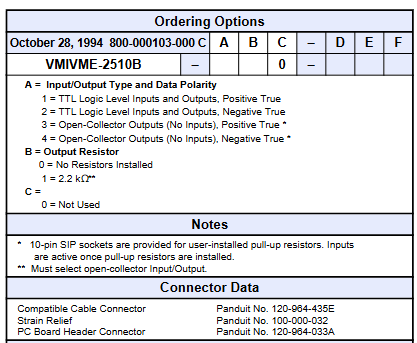
12 bit resolution, bipolar voltage output range can be selected as ± 2.5 V, ± 5 V, or ± 10 V; unipolar voltage output range can be selected as 0 to 2.5 V, 0 to 5 V, or 0 to 10 V.
The voltage output has a 10 mA load capacity within the full ± 10 V range, with optional 4 to 20 mA, 0 to 20 mA, or 5 to 25 mA current loop outputs.
The voltage output accuracy is 0.05%, and the current loop output accuracy is 0.08%. There are 4, 8, or 12 channel configurations to choose from.
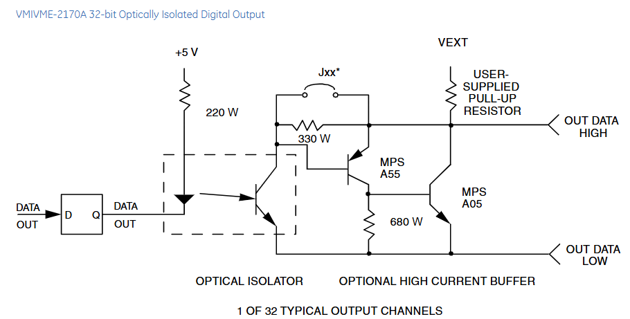
Using optical data coupling to provide complete galvanic isolation, static read back data registers simplify program control, and the front-end panel can be used for on-site connections.
The program controlled voltage output connection/disconnection operation facilitates system testing.
working principle
Internal functional structure
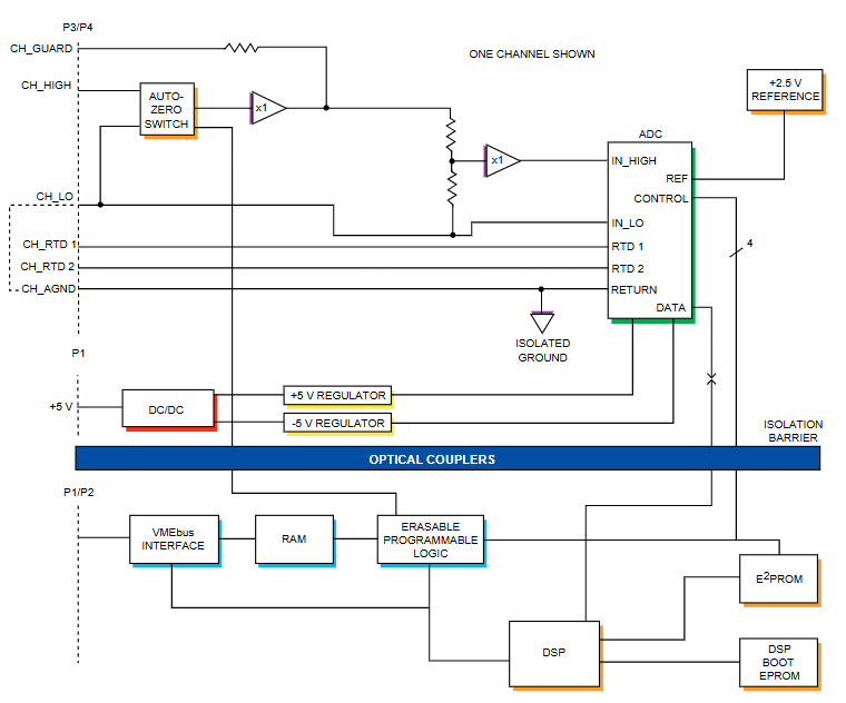
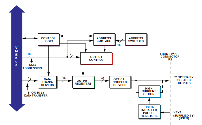
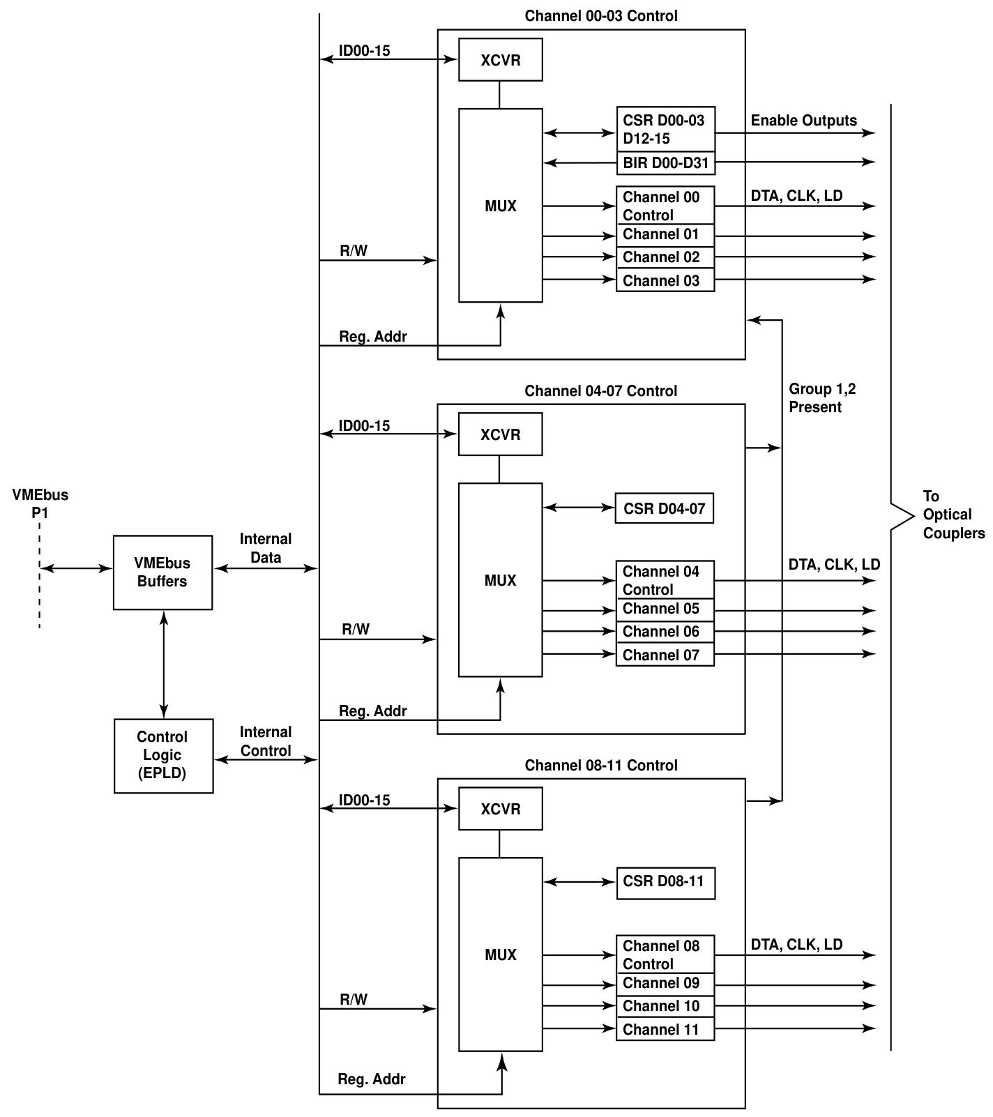
Composed of VMEbus interface, channel control, isolated analog output, and DC/DC power converter.
VMEbus interface: Communication with VMEbus is controlled by a single electrically programmable logic device (EPLD). Data and control registers are distributed in three channels to control the EPLD, respond to bus data transmission requests and control data flow, and generate data transmission acknowledgement (DTACK *) after completion of transmission.
Channel control: The data transmission control of the output D/A converter is divided into three identical 4-channel groups, each group is allocated and controlled by an EPLD, supporting optional configurations of 4, 8, or 12 channels. Each channel control EPLD contains four data registers, which receive channel data words from VMEbus and provide independent data serializers for each channel.
analog output channel
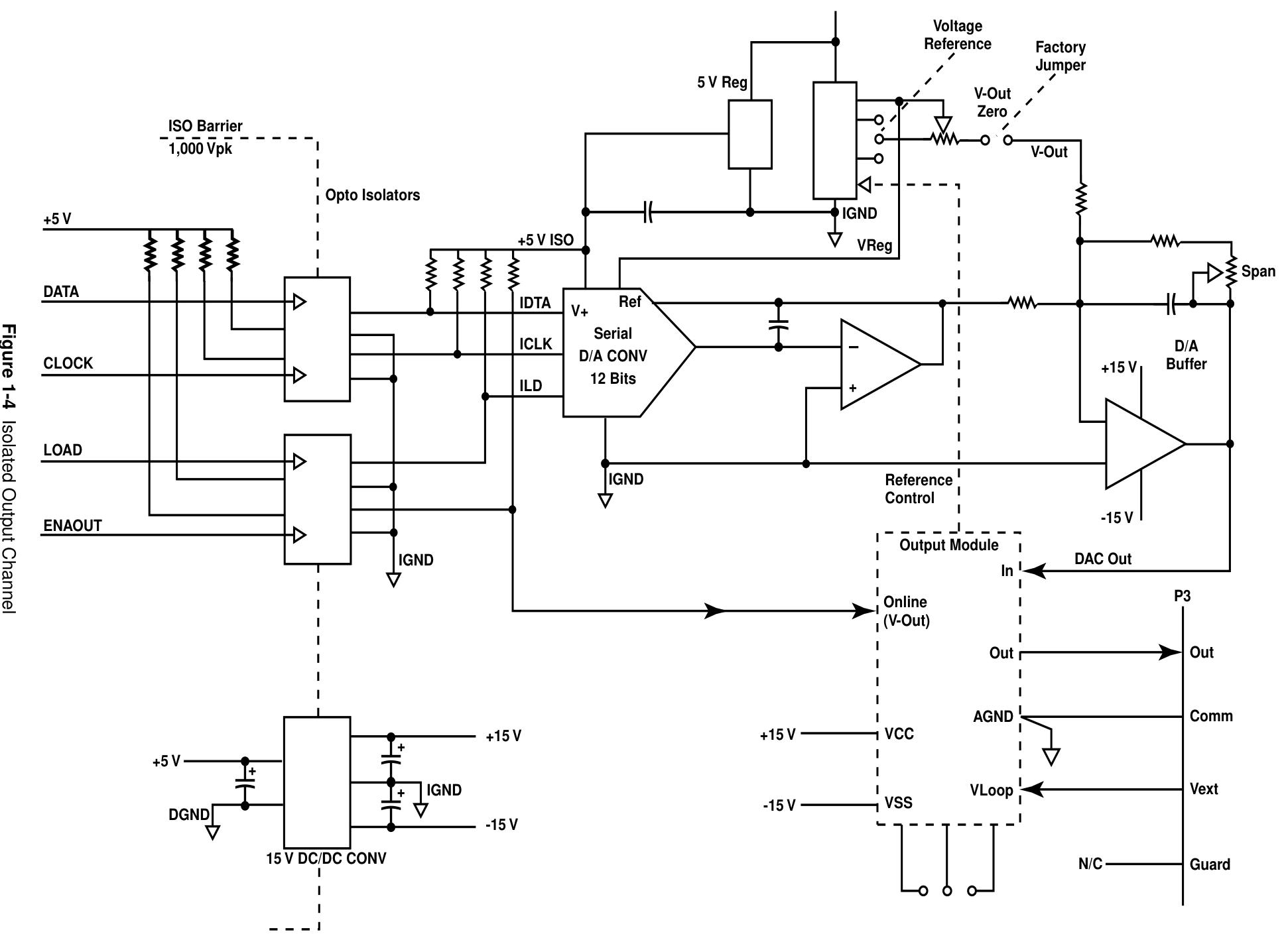
Isolation: Each output channel is isolated from VMEbus and all other channels through an isolated DC/DC converter and four optocouplers. The DC/DC converter provides ± 15 VDC isolated power supply, while the optocouplers isolate digital control signals.
Digital to Analog Conversion: A serial digital to analog (D/A) converter receives a 12 bit data word and generates a specific range of output voltage. The output module converts it to a specified voltage or current output according to the configuration.
Voltage and current output: All outputs are factory configured as unipolar voltage, bipolar voltage, or constant current. The voltage output module includes a unity gain buffer and an output switch, while the current output module includes a voltage current converter and a transmission transistor.
DC/DC power converter: Each channel contains a DC/DC converter that obtains isolated ± 15 VDC power from the VMEbus+5 VDC power bus to supply power to the isolated portion of the channel.
Configuration and Installation
Unboxing process
Some components are sensitive to electrostatic discharge, and unused boards should be stored in their original packaging. When placed on the workbench, it is recommended to insert conductive materials underneath. After receiving the goods, it is necessary to check whether there is any transportation damage. If there is, a claim should be made to the carrier and VMIC should be notified. When installing or removing the board, power off and insert the board correctly into the chassis slot.
run setup
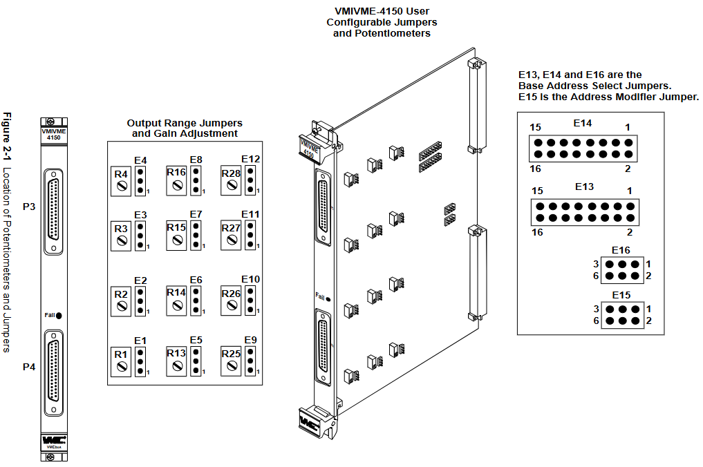
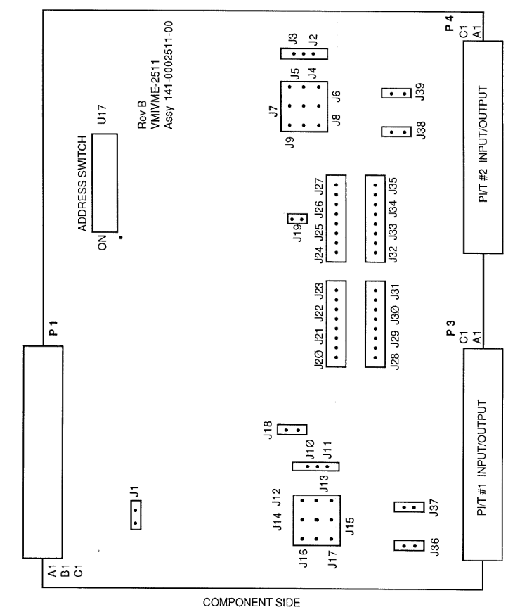
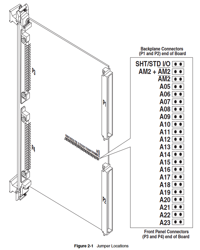
The board address and I/O access mode are controlled by replaceable jumpers on the board, including address modifier jumpers (E15), base address selection jumpers (E13, E14, E16), and output range selection jumpers. Different jumper configurations correspond to different functions and parameters.
Bipolar voltage output: It can be configured as 2.5 V, 5 V, or 10 V through user installed jumpers, and different channels correspond to different jumpers and adjustable potentiometers.
Unipolar voltage output: configurable for 0 to 2.5 V, 0 to 5 V, or 0 to 10 V, with corresponding jumpers and adjustment components.
Current loop output: Each channel has jumper wires that can be configured with internal or external power supply, supporting different current ranges.
calibration
Before leaving the factory, it has been fully calibrated. If recalibration is required, digital multimeters, card cages, expansion cards, resistors, and other equipment need to be prepared to calibrate the bipolar voltage output, unipolar voltage output, and current output according to specific steps. After calibration, appropriate sealing agents need to be used to re seal and adjust the components.
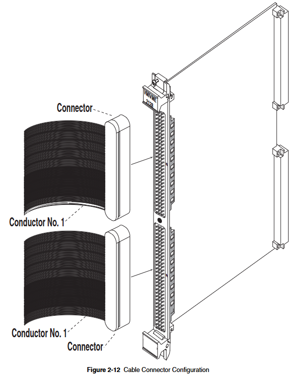
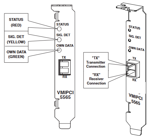
I/O cable and front-end panel connector configuration
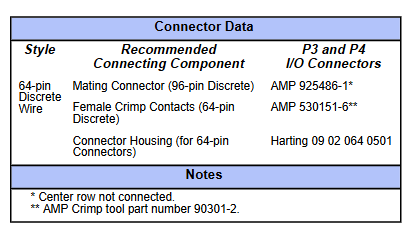
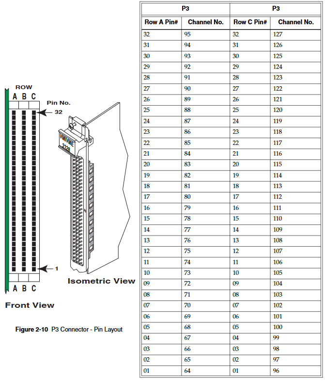
The front-end input connectors (P3 and P4) are standard ultra small 37 pin female D-shaped connectors with specific pin layouts and assignments, corresponding to different outputs and functions.
Programming
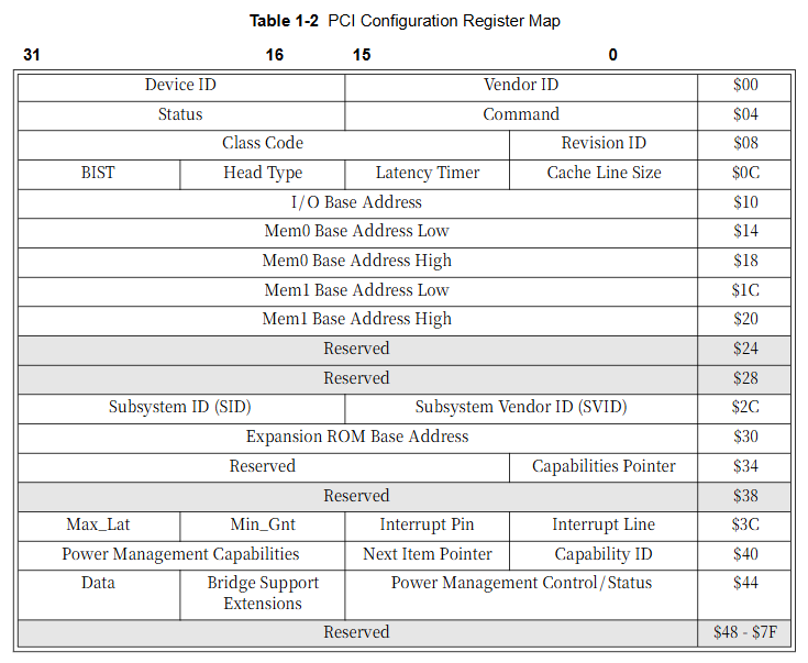
Register Mapping
Communication is carried out through 16 block control, status, data, and identification registers mapped to the A16 short I/O space or standard A24 data space, including board identification registers (BIR), control/status registers (CSR), output data registers (ODR), etc.
Board Identification Register (BIR): Contains the identification code (22 million hexadecimal) of the VMIVME-4150 board, located in the first two words of the board base address, and is read-only.
Control/Status Register (CSR): Provides control and monitoring of board functions, including output enable, output load cycle status, data encoding, self-test LED, etc. Each bit has specific functions.
Output Data Register (ODR): Each of the 12 analog outputs has a dedicated 12 bit output data register that supports read and write operations. The data is transmitted to the output D/A converter in a serial manner.
Reset operation
The system reset operation will reset all read and write registers to zero, causing the board to be in a specific state, such as analog output level, status, data encoding, and front-end panel LED status, all of which will change accordingly.
Analog output control
The output register and data format are controlled by CSR bit D12 and can be in offset binary format or binary complement format. The output range is determined by the jumper on the board, and the voltage output can be controlled by the bit in CSR to determine the connection status with the output connector. The data is transmitted from the output data register to the output D/A converter through an internal output load cycle, during which there is a corresponding busy flag indication.
maintenance
Provided information on product maintenance and upkeep, such as checking system power, software, configuration, connections, etc. in case of product malfunction. We do not recommend user level repairs. If you need to return the item, please contact VMIC to obtain a Return Merchandise Authorization (RMA) number. The drawings and tables in the manual are for reference only.