Call us 24/7uaedcs@163.com
Welcome to the official website of CNIACS Automation Technology Co., Ltd!
Call us 24/7uaedcs@163.com

GE VMIVME-1182 64 channel isolated digital input board

Basic characteristics

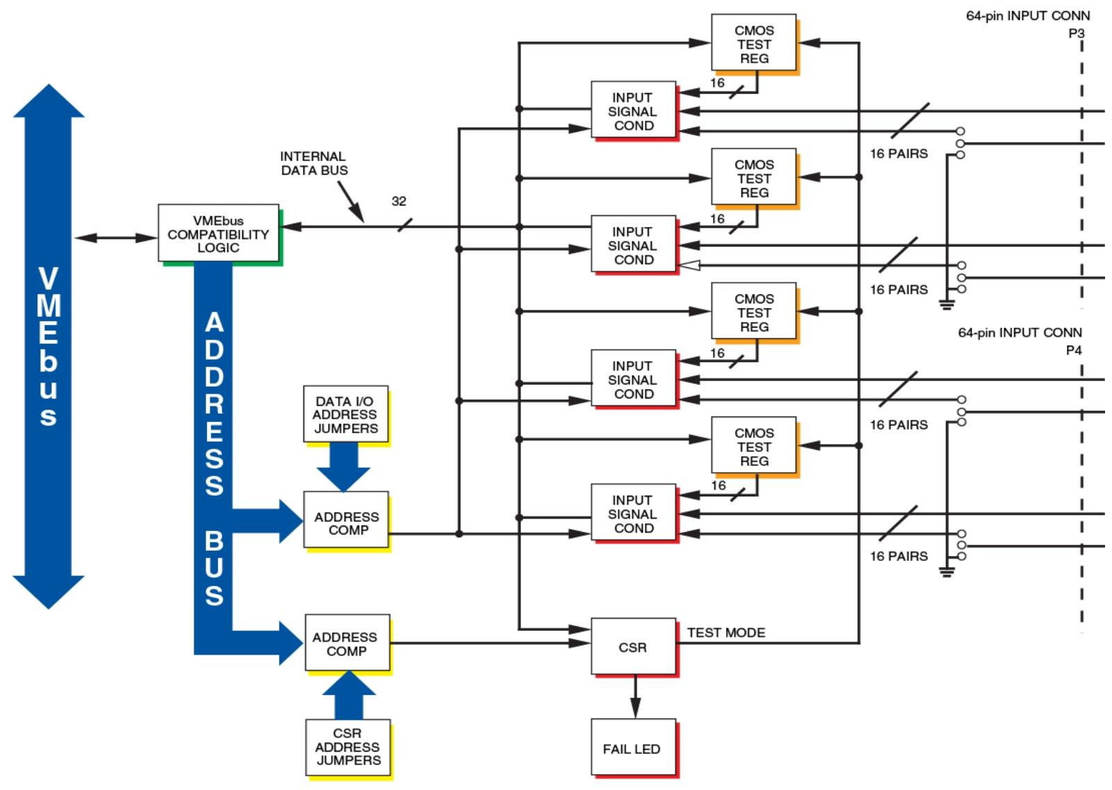
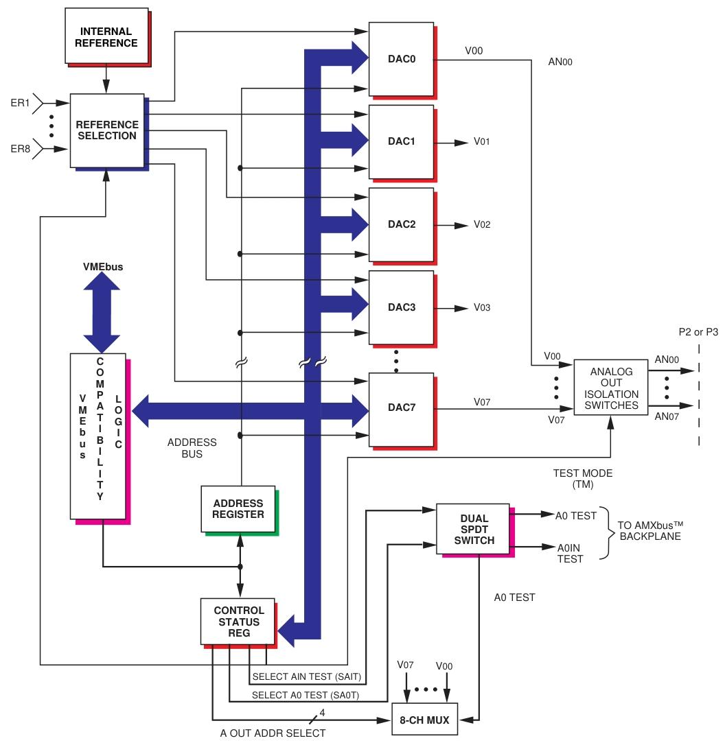
It has 64 optically isolated input channels and supports multifunctional operations for each channel, including monitoring of state changes (COS), sequence of events (SOEs), pulse accumulation, programmable debounce time, and time stamps.

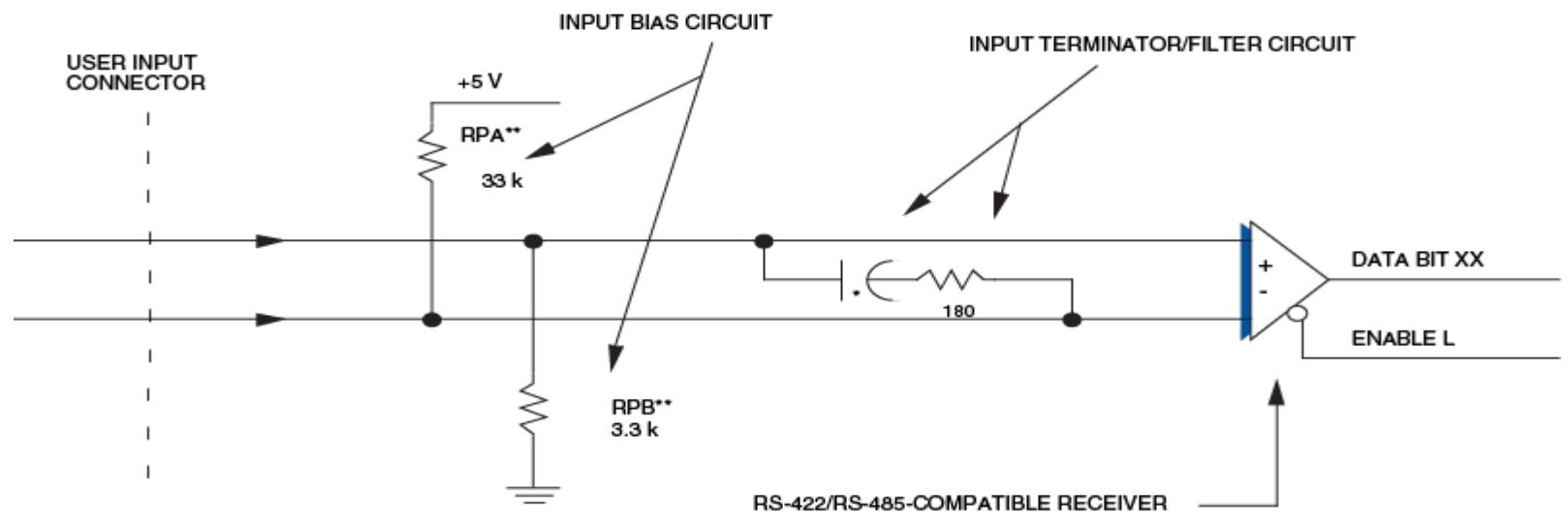
The input voltage range covers 5-250VDC or 4-240VAC, and the isolation between channels and between channels and VME bus can reach 1500VDC or 1100VRMS.

The pulse accumulation range is 0-65535 pulses, supporting channel by channel monitoring of SOEs. The debounce time and COS function can be controlled channel by channel through software.

The measurement interval is 1.0ms, and COS can be disabled, rising edge (low to high transition), falling edge (high to low transition), or triggered by any edge.

Supports short/standard, monitoring, non privileged, or arbitrary access modes, with user selectable interrupt levels, compatible with UIOC ®。

When used in conjunction with a matching suppression panel (such as VMIVME-3459), it complies with the ANSI/IEEE STD C37.90.1-1989 surge protection standard.

Application area 

Data acquisition system, nuclear power plant monitoring, control system, etc.

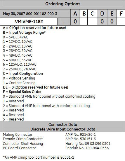
ordering information

The meaning of each parameter in the ordering options: A is a reserved option (0); B represents the input voltage range (0-7 corresponds to different AC and DC voltages); C is the input configuration (0 is voltage sensing, 1 is contact sensing); DE is a reserved option (0); F is a special sales order (0-5 corresponds to different panel configurations).

Discrete line input connector related information: The matching connector is AMP No.925486-1, the female contact point is AMP No.530151-6, the connector housing is Harting No.09 03 096 0501, the printed circuit board connector is Panduit No.120-964-033A, the AMP crimping tool model is 90301-2, and DC or AC can be selected through software.

Functional feature details

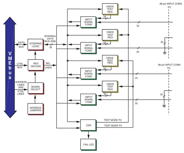
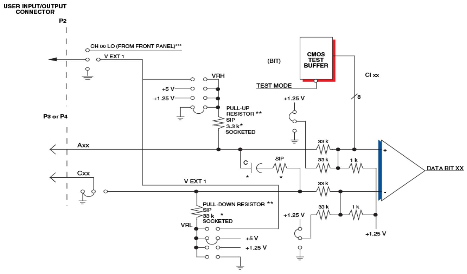
Basic functions: It can detect COS with 64 digital inputs, perform time tagging and counting. The onboard buffer can store COS information with time tags to analyze SOEs. The pulse accumulator is used to count COS. When COS is detected, it can be programmed to issue an interrupt, and each channel processes it independently.

COS timing: The input signal is latched every millisecond, and after a programmable debounce time (1.25ms-1.024s), if a valid COS is detected, it will be time marked and stored by a millisecond timer. The minimum reliable detection pulse time is 2ms.

COS detection: Programmable detection of rising edge, falling edge, or both, detecting COS can generate interrupts or disable.

Time stamping: Each COS event can be marked with a timer value of 0-65s, which updates every millisecond. When the maximum value is reached, it resets to zero and notifies the host.

Sequence of Events (SOE): SOE memory is allocated to two buffers (each capable of storing 3000 events), where the host processes one buffer while the other can load new event data. SOE logic can issue interrupts to the host at the end of the buffer or when the user sets a count.

Pulse Accumulation: Each channel has a Pulse Accumulation Count (PAC) register, and when the count reaches 65535, it will notify the user through a flag in the control register or issue an interrupt.

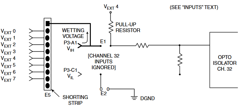
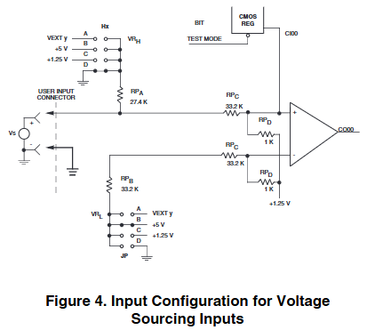
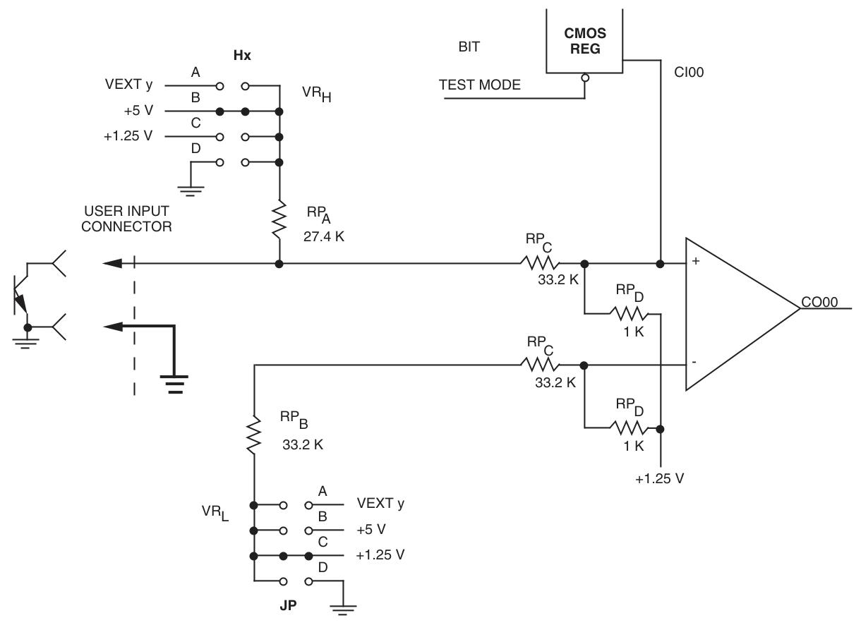
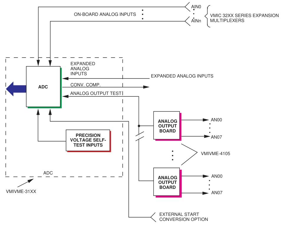
Input configuration: divided into voltage sensing and contact sensing options. The contact sensing option is equipped with a pull-up resistor to the wetting voltage pin, while the voltage source option has no pullups and has 8 wetting voltage input pins. Channel 32 can be changed to a wetting voltage supply through jumper wires.

Electrical specifications

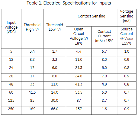
Provides high threshold, low threshold, contact induction (open circuit voltage, contact current), and voltage induction (source current) parameters corresponding to different input voltages (VDC), with a minimum inter channel crosstalk suppression of 80dB (1kHz) and a minimum common mode suppression of 80dB (DC-60Hz).

VME compliance

Compliant with the VMEbus specification (ANSI/IEEE STD 1014-1987, IEC 821 and 297), it provides response address modifiers, data access modes, and interrupt situations corresponding to different addressing modes.

Other characteristics

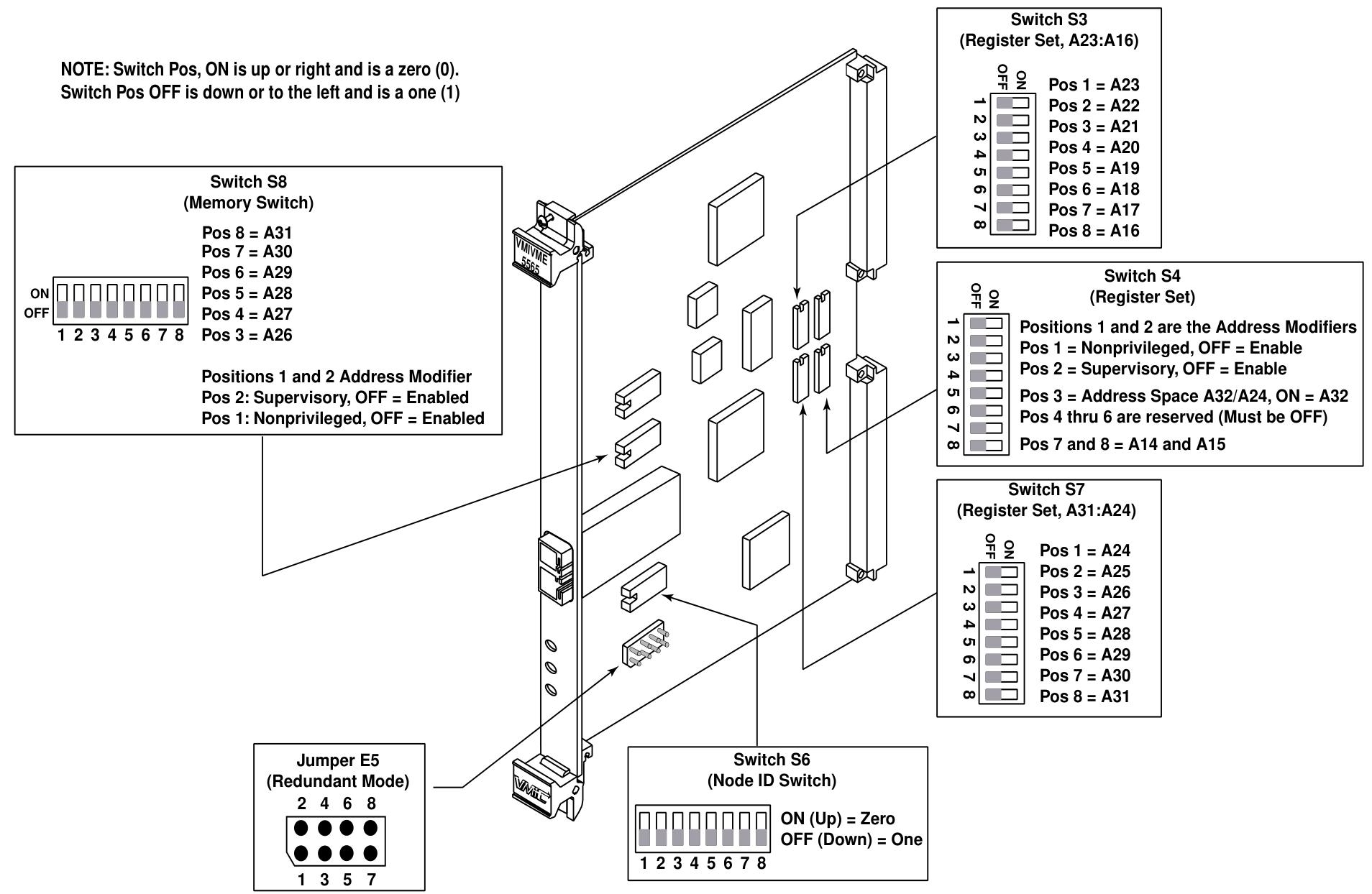
Board address: Set the basic VME address through jumper wires, with an address space of 8K words.

VME access: Address modifier bits are selected and decoded through jumpers, supporting non privileged, monitored, and both board access.

Self check: The system automatically runs after resetting, or it can be run by activating the test mode bit in CSR. The self check result is stored in the control register space, and the LED status does not change with the self check result. It mainly checks the integrity of the microcontroller and onboard memory.

System reset: After reset, there are default conditions such as input transmission (1ms debounce), LED lighting, and test mode activation.

Front panel status LED: It lights up after system reset and can be controlled by software switch.

Interrupt: It can be issued at any level, and after confirmation, the bus will place a single byte vector. There are multiple interrupt triggering conditions that can be enabled/disabled.

Physical/Environmental Specifications

Dimensions: Height 9.2 inches (233.4mm), Depth 6.3 inches (160mm), Thickness 0.8 inches (20.3mm).

Power requirement: Typical value of 2.0A at 5V, plus power consumption of pull-up resistor.

Cooling method: forced air cooling.

Temperature range: working 0-65 ° C, storage -25-85 ° C.

Altitude: Working at 0-10000 feet (3048m).

Humidity: Operating relative humidity of 20% -80%, non condensing.

Maximum weight: 0.7kg.

GE VMIVME-1128 128 bit high-voltage digital input board

Basic characteristics

Equipped with 128 bit high-voltage digital inputs, with 8 inputs per group, the monitoring voltage source or current sinking signal can be selected through jumper wires.

An open circuit can provide logic 0 or (jumper optional) logic 1.

Equipped with onboard built-in test (BIT) logic for fault detection and isolation, the front panel is equipped with a fault LED.

Users can choose the input voltage threshold (0.61 to 34V), with an input range of 0 to 66V (see Table 1).

Compliant with VMEbus specification Rev. C. 1, supports A24: A16: D32/D16/D08 (EO), from device address 39/3D: 29/2D.

Adopting a dual Eurocard shape (6U), equipped with high reliability DIN type I/O connectors, compatible with VMIC’s intelligent I/O controllers (VMIVME-90xx series) and universal I/O controllers (VMIVME-9300 series).

Application area 

Automatic testing equipment, control system input, data acquisition system, digital input status monitoring, universal digital input, low maintenance application (BIT), status sensor monitoring, monitoring system, etc.

Functional feature details

Compliance and Appearance: Compliant with VMEbus specifications (ANSI/IEEE STD 1014-1987, IEC 821 and 297), with an appearance of 6U.

Input connector type: Use two 96 pin female connectors. For large-scale termination (IDC), it is recommended to use ERNI IDC DIN connectors and 0.033-inch 30 AWG ribbon cables; For discrete lines, Harting connectors and related accessories are recommended, and any connector requires a housing with a fixed lever. Harting housing is recommended.

I/O organization: 16 input ports, each 8-bit wide, with a total of 128 inputs, addressable to any address within the short monitoring and/or short non privileged or standard monitoring data and/or standard non privileged data I/O mapping.

Addressing scheme: 32 bytes can be individually addressed on 8-bit, 16 bit, or 32-bit boundaries. There are board ID register, control and status register (CSR), and 16 input bytes on the board. 20 jumpers determine the base address of the board, and another jumper is used for standard or short I/O access, providing the relative position address mapping of each register.

Input circuit characteristics: The input is single ended, with a high input impedance (15k). The threshold accuracy is usually 10% in the input range of 3 to 66V, and ± 200mV in the input range of 0V to 3V. Please refer to the relevant charts and Table 1 for threshold levels.

Ordering information

ABC=000 in the ordering options (reserved for future use).

Provided descriptions and I/O connector models corresponding to different connector styles, as well as models of Harting crimping tools, and also provided contact information.

Built in testing (BIT)

The design has built-in testing logic, supports board level diagnostics, and can test all onboard active components. Provide special output registers for testing input circuits, controlled by the test mode bit in CSR. The fault LED on the front panel lights up when powered on, and can be turned off through program control after successfully completing user-defined diagnostic software.

Physical/Environmental Characteristics

Temperature range: storage -20 to 85 ° C, operation 0 to 55 ° C.

Relative humidity range: Non condensing 20 to 80%.

Altitude: Working up to 10000 feet.

Cooling method: forced air convection.

Size: Dual Eurocard (6U), 160 × 233.35mm.

Power requirement: Typical value of 2.31A at 5V, can be connected at the front panel (P3 or P4) or P2, VMIC provides recommended VMIAC-0129 P2 power accessories.

Mean Time Between Failures (MTBF): 228636 hours (30 ° C Bellcore method).

GE VMIVME-111 64 bit High Voltage Digital Input Board

Product Overview

VMIVME-111 is a 64 bit high-voltage digital input board with built-in testing capabilities, compliant with the VMEbus specification, and featuring a dual height European card design. It is suitable for scenarios that require monitoring multiple digital input signals and is compatible with the intelligent I/O controller series of GE Fanuc embedded systems. It supports hot swappable replacement and is software compatible with VMIVME-1110.

Core Features

Equipped with 64 bit differential or high-voltage digital input.

Each group of 32 inputs can be monitored through jumper selection: contact closure, voltage source, current absorption, or differential signal.

An open circuit can provide logic 0 or (jumper optional) logic 1.

Equipped with input filter options.

The onboard built-in testing logic is used for fault detection and isolation.

The front panel is equipped with a fault LED indicator light.

Users can choose to input a voltage threshold (1.25 to 66V).

Compatible with RS422/RS485 differential line receiver, providing ± 7V noise immunity.

Supports 8-bit, 16 bit, or 32-bit data transmission.

Adopting high reliability DIN type I/O connectors.

By using the corresponding suppression panel (such as VMIVME-3451), optical isolation can be achieved, which meets the surge protection requirements of ANSI/IEEE STD C37.90.1-1982.

Ordering Options

A=0 (option reserved for future use).

B is the input filter/terminator option: 0 is with input filter/terminator (the input filter/terminator circuit can provide a series RC terminator or input filter through jumper selection, with a time constant of 0.14ms, used for receivers compatible with RS422/RS485); 1 is without input filter/terminator; 2 is a 2 μ s filter; 3 is a 10 μ s filter; 4 is a 5ms filter; 5 is a 1ms filter.

C=0 (option reserved for future use).

Connector data

Compatible cable connector: Panduit No.120-964-435.

Strain relief: Panduit No.100-000-072.

Printed circuit board plug connector: Panduit No. 120-964-033A (also known as ITW/Pancon).

Functional characteristics

Compatibility: Compatible with VMEbus specifications, dual height appearance.

Input connector type: Dual 64 pin connector – DIN 41612.

I/O organization: 8 input ports, each 8 bits wide, addressable to any address within the short monitoring and/or short non privileged I/O mapping, control and status register (CSR) addresses can be independently selected.

Addressing scheme: 8 ports can be individually addressed on 8-bit, 16 bit, or 32-bit boundaries, 1 CSR can be addressed on 8-bit boundaries, and 13 jumpers provide unlimited short data I/O address mapping options.

Differential signal input characteristics: The common mode input voltage range is -30 to+66V, and the input sensitivity is ± 100mV within the common mode range of -7 to+12V. The input impedance is high (33k Ω).

Single ended signal input characteristics: high input impedance (33k Ω), threshold accuracy of 1% (typical value) across the entire 66V range.

Signal conditioning input filter terminator option: A board with input signal filtering circuit can be ordered. For differential input, the circuit consists of a series resistor and a capacitor, which are connected across the signal input terminals; For single ended inputs, this circuit provides users with the option to select an input debounce filter with a time constant.

Built in testing: Designed with internal self-test logic to test all active components, providing special output registers to generate 16 bit data words for health testing during real-time or offline operations. CSR provides special test mode bits to enable the output test registers to drive differential receivers. The front panel fault LED lights up when powered on and can be turned off under program control after successfully completing user-defined diagnostics.

Physical/Environmental Specifications

Power requirements:+5V, typical value 1.4A, maximum value 2.0A.

Cooling: forced air convection.

Temperature: Operating temperature from 0 to 55 ° C, storage temperature from -20 to 85 ° C.

Humidity: 20 to 80%, no condensation.

Mean Time Between Failures (MTBF): Please contact the factory.

Related products and applications

For inter channel optical isolation and surge suppression that comply with ANSI/IEEE STD C37.90.1-1982 (IEEE-472), please refer to VMIVME-3451 specification.

Threshold voltage

When R=3.3k Ω, the threshold voltage formula is

Vt=[(V−1.25)(.91)]+1.25

The Vt values corresponding to different voltages are as follows: 1.25V corresponds to 1.25V, 5V corresponds to 4.7V, 12V corresponds to 11V, 24V corresponds to 22V, 28V corresponds to 25.6V, 48V corresponds to 43.8V, and 66V corresponds to 60.2V.

When R=33k Ω, the threshold voltage formula is

Vt=[(V−1.25)(.51)]+1.25

The Vt values corresponding to different voltages are as follows: 1.25V corresponds to 1.25V, 5V corresponds to 3.2V, 12V corresponds to 6.7V, 24V corresponds to 12.9V, 28V corresponds to 14.8V, 48V corresponds to 25.1V, and 66V corresponds to 34.3V.

GE ACC-0603RC V7865 VME Rear Conversion Module

Product Overview

ACC-0603RC is a Rear Conversion Module (RTM) designed specifically to convert the I/O signals of V7865 from VME P2 connectors to standard I/O connectors. It complies with the EU Directive on the Restriction of Hazardous Substances (RoHS) (2002/95/EC current revision) and is only compatible with V7865 single board computers.

Function and Interface

Panel I/O access

A serial port connector (DB9) that supports RS232 and RS422.

Two standard USB 2.0 connectors.

Digital Visual Interface – Digital (DVI-D) video support.

A Serial ATA (SATA) connector.

On board I/O access

A PIM I/O interface.

A SATA connector.

Installation

The ACC-0603RC RTM is installed at the rear of the VME chassis through a P2 connector. All signals are transmitted from the single board computer (SBC) installed at the front of the chassis to the P2 connector of the ACC-0603RC through the backplane, and should be installed in a chassis that supports the VME five row backplane connector.

Details of connectors, fittings, and switches

VME connector (P2): A standard VME64 five row connector used to route all signals from the backplane to the ACC-603RC connector, with a detailed pin allocation table.

COM2 connector (P6): Provides a serial port compatible with 16550, used through a standard DB9 connector, hardware can be configured as RS232 or RS422, supports baud rates up to 115 Kbaud, and has corresponding pin assignments (in both modes).

COM2 mode connectors (E1 and E2): Users can configure the COM2 mode, with different jumper settings corresponding to RS232 mode and RS422 mode. The default setting is bold display.

COM2 Terminal Switch (S1): Used to set the RS422 COM2 port mode for the terminal. When the switch is closed, the terminal is enabled, and when it is opened, it is disabled. Both switches must be in the same state at the same time, and the default setting is bold display.

USB connectors (J2 and J3): Adopting industry standard four position (conductor) shielded connectors with corresponding pin assignments.

DVI-D connector (J1): Provides high-speed digital connection, only transmits digital data, and has a detailed pin allocation table.

Serial ATA connectors (P4 and J15): support two SATA ports, one located on the panel (single shielded) and one located on the board (single unshielded), with scalability, specific wiring methods, and performance characteristics, and corresponding pin assignments.

PMC I/O PIM connectors (J10 and J14): Provide standard PIM connectors for routing PMC I/O from V7865 to universal modules on ACC-0603RC, with their own pin allocation tables.

Maintenance

If GE Fanuc embedded system products experience malfunctions, it is necessary to check software, system configuration, electrical connections, jumper or configuration options, card insertion status, connector pin cleanliness, interference with other components, and cable and I/O connection quality. If you need to return the product, please contact GE Fanuc Embedded System to obtain a Return Material Authorization (RMA) number. User level repairs are not recommended, and the drawings and charts in the manual are for reference only.

GE V7865 Intel ®  Core ™  Duo Processor VME Single Board

Product Overview

V7865 is the flagship Core Duo VMEbus single board computer of GE Fanuc embedded system, based on Intel Core Duo processor, which can provide processor and I/O flexibility to meet various application needs. It has three environmental versions: commercial, extended temperature, and reinforced extended temperature, which are very suitable for advanced defense, aerospace, and homeland security applications.

Core Features

Using Intel Core Duo processor with a speed of up to 2.0 GHz.

Maximum 3 GB DDR2 SDRAM memory.

Compliant with RoHS standards.

Up to 2 GB can boot CompactFlash.

667 MHz system and memory bus.

Compliant with ANSI/VITA 1.5-2003 (2ESST, up to 320 MB/s).

Optional VITA 41.3 (1000 Mb/s IEEE 802.3).

Two RS232/422 serial ports.

A PCI-X PMC site.

Four USB 2.0 ports.

Supports multiple operating systems.

Specification parameters

processor

Intel Core Duo processor, with a core processor speed of 1.6 GHz or 2.0 GHz.

High performance and low power consumption.

2 MB advanced level 2 cache.

667 MHz system bus.

SDRAM

The maximum memory configuration is 3 GB DDR2 SDRAM.

Onboard 1 GB of memory.

2 GB SODIMM (a 200 pin SODIMM DDR2 module).

The reinforced expansion temperature option is only available when the onboard memory is 512 MB or 1 GB.

CompactFlash

Maximum 2 GB CompactFlash.

CompactFlash can be configured as a boot device through BIOS boot device settings.

BIOS: V7865 system BIOS and video BIOS are provided in reprogrammable memory.

Gigabit Ethernet

VITA 41.3 (dual 1000 Mb/s).

Route dual gigabit Ethernet to the RJ45 connector on the front panel.

The Ethernet controller is Intel 82571.

USB port

Four USB 2.0 ports: two through P2 to Rear I/O, and two to the front panel.

The supported USB features include: isochronous data transfer, asynchronous message passing, self identification and configuration of peripheral devices, and dynamic (hot) connections.

VMEbus backplane interface: Tundra Tsi148 supports ANSI/VITA 1.5-2003 (2eSST) protocol, providing 320 MB/s bandwidth over the entire length of the 21 slot backplane, significantly improving performance compared to other buses, and also supporting broadcast mode. Optional VITA 41.3.

serial port

Two serial ports compatible with 16550, connected via DB-9 connector: one through P2 to Rear and one to the front panel.

The port has an independent 16 byte FIFO and supports baud rates up to 115 Kbaud.

Serial ATA: A serial ATA interface is connected through the VMEbus backplane connector P2.

PMC Expansion Slot: One 133 MHz PCI-X PMC site.

programmable timer

Two 16 bit timers and two 32-bit timers.

Map to PCI memory space.

Completely programmable through software and capable of generating PCI bus interrupts.

watchdog

Programmable interval.

Interrupt and board reset trigger.

size

6U (4HP) single slot European card shape.

Height: 9.2 inches (233.4mm).

Depth: 6.3 inches (160mm).

Thickness: 0.8 inches (20.3mm).

Power requirements

+5 VDC (± 5%), typical value to be determined, maximum value to be determined.

+12 VDC (± 5%), 0 mA.

-12 VDC (± 5%), 0 mA.

Airflow: Forced air cooling is required, and the minimum airflow measured at the top (outlet) of the equipment is 400 LFM.

temperature

Commercial: 0 ° C to 55 ° C.

Extended temperature: -40 ° C to 70 ° C.

Reinforced expansion temperature: -40 ° C to 70 ° C (Vita 47 Class EAC6).

humidity

Work: Relative humidity of 5% to 95%, no condensation.

Storage: Relative humidity of 5% to 95%, no condensation.

Impact: 20 g impact (reinforced expansion temperature).

Vibration (Reinforced Extended Temperature)

The PSD increases by 3 dB/octave from 5 Hz to 100 Hz.

100 Hz to 1000 Hz PSD=0.04g ²/Hz.

Reduce PSD by 6 dB/octave from 1000 Hz to 2000 Hz.

Ordering Options

V7865-210021: 2 GHz processor, 1GB DDR2 SDRAM, commercial temperature.

V7865-210026: 2 GHz processor, 1GB DDR2 SDRAM, reinforced expansion temperature.

Hardware accessories

ACC-0602:3U Rear Conversion Board.

ACC-0603:6U Rear Conversion Board.

GE MVME5500 series VME single board computer

Product Overview

The MVME5500 series is the latest flagship product of Motorola’s VME product line. It is a high-performance VMEbus single board computer (SBC) that uses the latest MPC7455 processor and can run at speeds of 1 GHz and above, making it ideal for data intensive applications. It not only provides faster processor performance, but also achieves balanced performance in terms of processor, memory, local bus, and I/O subsystems, enabling higher levels of performance in a single VMEbus slot, meeting the needs of original equipment manufacturers (OEMs) in markets such as defense and aerospace, industrial automation, and medical imaging. At the same time, it provides customers with migration paths to upgrade from multiple legacy boards.

Core Features

Processor and Cache: Equipped with MPC7455 processor, with a speed of 1 GHz or above, 256KB on-chip L2 cache and 2MB L3 cache, and equipped with AltiVec coprocessor, suitable for high-performance computing applications.

Memory: Onboard 512MB SDRAM with ECC, expandable by an additional 512MB through a memory mezzanine card, with a total memory capacity of up to 1GB.

Storage: 40MB flash memory (32MB soldered, 8MB slot style), 32KB NVRAM (4KB available for users).

Bus and Expansion: Dual PCI bus and dual PMC sites, with a bus speed of up to 66 MHz; 64 bit PCI expansion mezzanine connector, capable of supporting up to four additional PMCs.

Network interface: Gigabit Ethernet interface and 10/100BaseTX Ethernet interface.

Compatibility: Compatible with MVME51xx series I/O, even if fully configured with two PMC modules or one PMC module and an additional memory mezzanine, it only occupies a single VME slot and supports multiple migration paths and different P2 I/O modes.

Firmware and Software: Equipped with innovative firmware (MotLoad), supporting multiple operating systems and kernels, providing relevant libraries and built-in testing software.

Detailed specifications

processor

Microprocessor: MPC7455

Clock frequency: 1 GHz

On chip L1 cache (instructions/data): 32KB/32KB

On chip L2 cache (instructions/data): 256KB/256KB

L3 cache: 2MB

System Controller: Marvel Discovery GT-64260A

Main Memory

Type: PC133 ECC SDRAM

Speed: 133 MHz

Capacity: 512MB onboard, expandable to 1GB with additional memory mezzanine card (if PMC module is inserted into PMC slot 1, memory mezzanine card cannot be used)

Configuration: Two groups totaling 512MB

flash memory

Type: EEPROM, onboard programmable

Capacity: 8MB (via two 56 pin TSOP slots); 32MB soldered flash memory

Write protection: 32MB surface mount flash memory can be protected by jumper write protection

NVRAM

Capacity: 32KB (4KB available for users)

Battery life: 50 years at 55 ° C

Battery capacity life: 5 years at 25 ° C and 100% duty cycle

Replaceable battery: Yes

Counter/Timer

TOD clock device: M48T37V

Real time timer: 8 32-bit programmable timers

Watchdog Timer: Reset upon timeout

VMEbus interface: compliant with ANSI/VITA 1-1994 VME64 (IEEE STD 1014), with multiple controller functions and interrupt handling capabilities.

Ethernet interface

Port 1: Intel 82544EI Gigabit Ethernet Controller, speed 10/100/1000Mb/s, connected via front panel RJ-45.

Port 2: Controller integrated into the GT-64260A system controller, with a speed of 10/100Mb/s, connected via RJ-45 on the front panel or optional routing to RJ-45 on P2 and MVME761.

Asynchronous Serial Port

Controller: Two TL16C550C UART

Number of ports: Two, compatible with 16550

Maximum asynchronous baud rate: EIA-232 is 38.4K, originally 115Kb/s

Connector: Route to front panel RJ-45; One for development use on a flat surface

PMC interface and extensions

Dual IEEE P1386.1 PCI mezzanine card slots, supporting multiple address/data formats, bus clocks, and module types.

PCI expansion connector, supporting specific address/data formats, bus clocks, etc.

Power requirements: Excluding the power required for PMC or IMPC modules, specific parameters to be determined; The IPMC module will add additional power load.

Size: Multiple size parameters, such as 233.4 mm (9.2 in.), 160.0 mm (6.3 in.), etc.

Synchronous serial port: Different IPMC modules have different configurations, with varying parameters such as controller, number of ports, and baud rate.

Parallel port: The controller is PC97307, 8-bit bidirectional, fully supports IEEE 1284, compatible with Centronics (EPP and ECP are not included on MVME712M), only in main mode.

Compatibility and Migration

Backward compatibility: Continuing the direction of the Motorola MVME5100 series, it provides a migration path to a single platform for embedded controllers and single board computers, simplifying multiple requirements.

P2 I/O mode: Supports two types of jumper configurations for P2 I/O mode (PMC mode and IPMC mode), each with different compatibility and functionality.

IPMC module: IPMC761 and IPMC712 are optional additional PMC modules that provide backward compatibility with previous generation Motorola products and support multiple interfaces.

Conversion module: MVME761 and MVME712M conversion modules provide access to multiple standard connectors, supporting different interfaces and configurations.

Firmware and software support

Firmware Monitor: Motorola’s MotLoad firmware has extended features such as interrupt driven I/O, more comprehensive power on testing, and provides a debugger interface similar to “BUG”.

Operating System and Kernel: Supports WindRiver Systems VxWorks and MontaVista Linux Professional Edition.

Library: MPI Software Technology’s VSI/Pro VSIPL library can be used on MVME5500.

Built in testing software: Provides Motorola Built in Testing (MBIT) software, available in board level and system level versions, with multiple functions and APIs.

Order Information

MVME5500-0161 1:1 GHz MPC7455 processor, 512MB SDRAM, Scanbe controller

MVME5500-0163:1 GHz MPC7455 processor, 512MB SDRAM, IEEE controller

RAM5500-007:512MB memory mezzanine expansion card

GE CPCI-7055RC PowerPC ®  CompactPCI ®  single board

Product Overview

CPCI-7055RC is a single slot CompactPCI single board computer (SBC) equipped with a 750GX PowerPC processor that provides excellent processing performance, robustness, reliability, flexibility, and system characteristics to meet the most demanding requirements of embedded computing applications. It adopts the next generation of Marvel ®  Discovery ™  III chipset, equipped with rich interfaces and expansion functions.

Core Features

The processor speed can reach up to 1.0 GHz.

The working temperature range is from 0 ° C to+55 ° C.

Up to 1 GB DDR 400 SDRAM.

Up to 2 GB of CompactFlash.

Three independent 10/100/1000BaseTX Ethernet ports.

Supports Ultra DMA IDE controllers.

64 bit/66 MHz CompactPCI bus interface.

User programmable watchdog timer.

Equipped with passive radiator.

Support VxWorks ®  And Linux ®  Operating system.

Compliant with RoHS standards.

It has two PMC expansion sites (64 bit/100 MHz PCI-X, backward compatible with 5V, 33 MHz PCI).

Three high-performance serial ports.

Supports multiple PICMG specifications and provides system level flexibility.

On board temperature and voltage monitoring can be accessed through software to achieve application related environmental solutions.

Specification parameters

CPU:IBM 750GX PowerPC 1.0 GHz, Equipped with 1 MB of advanced level 2 cache, utilizing the next-generation Marvel PowerPC chipset, and integrating 2 MB of SRAM.

SDRAM: Up to 1 GB DDR 400 SDRAM with ECC.

CompactFlash: up to 2 GB.

Ethernet: Three dedicated 10/100/1000BaseTX Ethernet ports, one via RJ45 port on the front panel, and two can be connected via PICMG 2.16 or CompactPCI J3 backplane.

PMC Expansion: Two 64 bit/100 MHz PCI-X PMC expansion sites, backward compatible with 5V and 33 MHz, supporting dual width PMC, compliant with IEEE 1386.1 standard.

Serial interface: Three high-performance serial ports, two of which support asynchronous RS232/422/RS485 on the rear I/O J3, and one RS232 serial port with RJ45 connector on the front panel.

Other interfaces: One serial port on the front panel, and two additional ports through the CPCI J3 connector; Support IDE and hard drive; Front panel hardware reset; User programmable watchdog timer; Front panel status LED.

PICMG compliance: Supports Intelligent Platform Management Interface (IPMI) architecture (PICMG 2.9 Rev. 1.0), high availability hot swappable (PICMG 2.1 Rev. 2.0), and universal signal support (PICMG 2.0 Rev. 3.0).

Front panel status LED: Main IDE interface activity, board status, power supply, hot plug, LAN activity (located on each RJ45).

Operating system support: Linux, VxWorks.

Power requirements:+3.3 VDC (± 5%) typical 1.7A, maximum 3.04A;+5 VDC (± 5%) typical 3.2A, maximum 6.0A; ± 12 VDC (± 5%) maximum 50 mA.

Environmental specifications: operating temperature from 0 ° C to+55 ° C; storage temperature from -25 ° C to+80 ° C; relative humidity from 10% to 90%, no condensation.

Shock: 10 Gs, 16 ms half sine wave, 6 axes, 10 pulses per axis.

Vibration: 6 Gs RMS (20-2000 Hz) random, 0.0185 G2 per Hz spectrum.

MTBF:361, 616 hours.

Size: 6U single slot European style card with a height of 9.2 inches (233.4 mm), depth of 6.3 inches (160 mm), and thickness of 0.8 inches (20.3 mm).

Order Information

VMICPCI-7055RC-32×100:6U cPCI SBC – 1 GHz 750GX,1 GB DDR SODIMM, No CompactFlash, via J3 Ethernet, 2x PMC, 64 MB boot flash, 32 KB NVRAM, 3x serial ports, compliant with RoHS standards.

VMICPCI-7055RC-31×100:6U cPCI SBC – 1GHz 750GH,512 MB SODIMM, No CompactFlash, via J3 Ethernet, 2x PMC, 64 MB boot flash, 32kb NVRAM, 3x serial ports, compliant with RoHS standards.

VMIAC-7055RC-000: The rear conversion module of PCI-7055 complies with RoHS standards.

GE VMIVME-3125 Analog Input Board

Product Overview

VMIVME-3125 is a flexible and low-cost analog input board that adopts the VMEbus 6U single height format and provides 16 differential or 32 single ended analog input channels. The channels are digitized using a 12 bit resolution analog-to-digital converter (ADC). This board does not require software settings, and will automatically start scanning all input channels after power on or system reset. The converted data is stored in dual port memory and can be accessed immediately through VMEbus. It also has a built-in self-test (BIT) function, and the input voltage range and gain can be programmed by the user through jumper wires. The VMEbus base address and access mode can be fully selected.

Core Features

16 differential or 32 single ended analog input channels.

1 12 bit A/D converter with built-in tracking and holding function.

All inputs are automatically scanned at a total rate of 40 kHz.

Scanning can begin without software initialization.

The input range is from ± 50 mV to ± 10 VDC.

Input overvoltage protection, analog input is low-pass filtered at 50 kHz, and an optional 40 Hz low-pass filter sub board can be added.

Supports discrete or large-scale terminated cables.

Input pull-down resistor to prevent input floating.

Supports both online and offline built-in testing (BIT).

The programmable gain of the jumper is x1, x10, x100.

The optional A/D range is ± 5 VDC, ± 10 VDC, and 0 to 10 VDC.

Data access methods: D16, D08 (EO), D08 (O).

Front panel LED indicator light.

1000 VDC isolation between analog ground and digital ground.

Optional 0-20, 4-20, and 5-25 mA current input ranges.

Working principle

Functional components: mainly including VMEbus interface, analog-to-digital converter (ADC) and control logic, analog input multiplexing, gain and conversion, BIT voltage reference and multiplexer, board ID register and other functional parts.

VMEbus interface: Communication registers are mapped to 64 16 bit words (128 bytes) in memory, which can be located on any 128 byte boundary within the VMEbus short I/O space and can be configured to respond to short monitoring or short non privileged data access.

Analog to digital conversion control and timing: There are two operating modes, namely continuous scanning of all 16 or 32 analog input channels, and stopping scanning and locking to a single channel. Using a 12 bit ADC with a conversion time of 8.5 μ sec, the channel acquisition cycle is once every 25 μ sec, and the total scanning rate is 40 kHz. The ADC’s built-in tracking and holding device can prevent erroneous readings from signals that change during the conversion cycle.

Built in Test Reference: Equipped with programmable precision voltage reference for board built-in testing (BIT). When selected, the BIT voltage is fed to the ADC through a programmable gain amplifier, bypassing the external analog input on channel 0. Users can enable BIT during initial board installation or real-time system self diagnosis.

Analog Input: The front panel connector provides 16 differential or 32 single ended analog inputs. It is recommended to use differential mode to reduce noise and improve common mode rejection ratio. Unused inputs should be grounded, and the low end of the differential input on the board has an internal 22 M Ω pull-down resistor.

Low pass filter: Provides a passive single pole low-pass input filter with a normal -3 dB cut-off frequency of 50 kHz, and can also be configured with an additional sub board to provide a low-pass filter with a cut-off frequency of 40 Hz.

Input multiplexer: There are two levels of analog multiplexing, with each of the 32 inputs selected through one of the four 8×1 first level analog input multiplexers. The second level multiplexer is configured as a 4×2 board, and one or two of the first level output signals are selected to provide single ended or differential operation mode. BIT reference voltage can also be selected.

Programmable gain instrumentation amplifier: After selecting the input channel and passing through the input multiplexer, it enters the programmable gain amplifier as a differential input. The differential amplifier suppresses common mode noise and delivers the scaled single ended output to the ADC. The hardware can jumper the gain to 1, 10, and 100.

Channel sequencer and dual port RAM memory: typically run in scan mode, starting conversion immediately after power on or reset. After A/D conversion is completed, the dual port control logic retrieves the conversion data and stores it in the corresponding dual port register of the channel. The channel counter increments and selects the next channel to be multiplexed to the ADC. After all input channels are converted and stored, the channel counter resets and starts the channel scanning sequence again. The channel sequencer can be stopped at the current address by the stop auto scan bit in the control/status register.

Board ID Register: The first position of the VMIVME-3125 register group is the read-only board ID register, with a value of $37, used for general system software to automatically determine the installed board.

Built in power converter and ADC power supply: The power supply for the analog circuit is provided by an onboard DC-DC converter, which converts the+5 VDC of VMEbus to a regulated ± 15 VDC. The+5 VDC logic power supply for the ADC is provided by an onboard regulator, and a separate+5 V DC-DC converter is used to provide isolated analog ground for the ADC.

Configuration and Installation

Unpacking procedure: Components may be sensitive to electrostatic discharge. When handling, the board should be placed on conductive material. After unpacking, check for any transportation damage. If there is any damage, file a claim with the carrier and report to GE.

Physical installation: Power off installation, insert the board into the appropriate slot of the chassis, ensure correct alignment and orientation, smoothly slide towards the mating connector until firmly seated.

Jumper installation

Board address: occupies a short I/O address space of 128 consecutive bytes, with the base address controlled by jumper E6 to E14. The installed jumper corresponds to binary 0, and the uninstalled one corresponds to binary 1. The factory default address is short I/O $0000 (all jumper installations).

Address modifier: Jumper E16 determines the access mode of the response, including monitoring, non privileged, or both.

Input configuration: Three jumpers (J4, J5, and E5) are used to configure single ended or differential inputs, two jumpers (E1 and E2) control the input voltage range, two jumpers (E3 and E4) control the gain, and there are filter related jumpers. The factory default configuration is single ended, ± 10 V range, and unity gain.

Analog input connector description: 16 differential or 32 single ended analog input connections are made through the front panel 37 pin D-type connector P3, with corresponding pins and signal allocation.

Calibration Procedure: To obtain the specified accuracy of analog measurements, calibration is required for the required range and input topology. Firstly, instrument amplifier offset and BIT voltage calibration are performed, and then the corresponding offset and gain calibration procedures for the input topology are selected. Calibration requires a 5-digit digital voltmeter (DVM) and precision voltage reference equipment.

Programming

Memory mapping: occupying 128 bytes of address space, including four information and control registers, as well as a conversion data register. Depending on the jumper configuration of the board (single ended or differential input, normal or maximum buffer for differential input), there are different memory mapping tables.

Register description

Board ID register: 8-bit read-only register, offset $00, value $37, used to uniquely identify the board.

Configuration register: 8-bit read-only register, offset $01, indicating the current configuration, including input mode and filter bandwidth information.

Control/Status Register: 8-bit read/write register with an offset of $02, allowing software to control the board and indicate its current status, including functions such as stopping automatic scanning, maximum buffer, complement, mode bit, LED off, etc.

Channel pointer register: an 8-bit read-only register with an offset of $03, typically storing the input channel number currently being sampled and converted. Under specific configurations, it can determine the most recently updated data register.

Data registers: Depending on the state of the maximum buffer location, there are 16 or 32 data registers. Starting from an offset of $40, each 12 bit conversion data containing its related channel is aligned to the right within the 16 bit data register.

Built in testing function: It can test the function by applying various internal reference voltages to channel 0 input. The host software can read the value of channel 0 and compare it with the expected value. There are corresponding BIT value tables for different ranges and gain settings.

Range and gain determination: The analog gain and range can be set by the user, but the software cannot directly read these settings. It is not recommended to determine the current settings through BIT voltage stimulation, as the board must be calibrated to a single gain and range setting.

Accessing data in byte form: Data registers should typically be accessed using a single 16 bit word transfer, or two consecutive byte transfers, but there is a risk of confusion caused by data updates, which can be avoided by pausing automatic scanning or ensuring that byte accesses are continuous and undisturbed.

Current input options: VMIVME-3125-200 and VMIVME-3125-300 offer different terminal resistances, and the ADC input voltage is related to the current range, allowing for the calculation of the current signal through a formula.

GE VMIVME-4105 8-Channel 12 Bit Multiplicative Digital

Product Overview

VMIVME-4105 is an 8-channel 12 bit multiplication analog-to-digital converter board that uses a dual European card (6U) format and comes with a front panel fault LED indicator. It is compatible with the VMEbus specification and needs to be paired with VMIVME-31xx to implement built-in testing functions. It is suitable for scenarios that require multi-channel analog output.

Core Features

Channels and outputs: 8 multiplication analog output channels, the output can be selected to P2 or the front panel (P3 connector) through jumper wires, supporting output ranges of ± 10 V or 0 to -10 V, selected through jumper wires.

Resolution and multiplier: 12 bit resolution, supports 2-quadrant or 4-quadrant multipliers, can be selected through jumper wires.

Reference voltage: Supports 8 independent or 1 shared AC or DC voltage references, which can be selected through jumper wires. There is an internal DC reference to support built-in testing.

Test mode: compatible with other VMIC boards and VMIC AMXbus ™ The backplane is used for fault detection and isolation, with two dedicated analog buses. During testing, 8 DAC outputs can be isolated from the P3 connector to avoid affecting user device connections. However, real-time fault detection and isolation are not supported when using the multiplication DAC option, and built-in testing is not supported when using the P2 output.

Simulation test mode: Any 8-channel analog output can be switched to the simulation test bus (Test Bus 1 or Test Bus 2), which is used to verify the multiplexer expansion board and each DAC channel of the VMIVME-4105 board through the ADC board.

Functional characteristics

Simulated output equation

Unipolar operation (two quadrant multiplier): V OUT=- V REF 4096 (DigitalCode 10)

Offset binary bipolar operation (four quadrant multiplier):

V OUT=−V REF+V REF 4,096(DigitalCode 10)×2

Board address: Select through a 12 bit DIP switch, decode VMEbus address lines A04 to A15 for board selection.

VMEbus access: decode address modification bits to support non privileged short I/O or monitoring short I/O access, selected through a single jumper.

Data transmission: During write operations, the data destination is controlled by data bit 15. When bit 15 is 1, it is written to the control register, and when it is 0, it is written to the addressed digital to analog converter (DAC); Read any valid board address to read the board status. The digital data of the DAC is contained in data bits D00 to D11. Unipolar operation uses unipolar binary code, and bipolar operation can use offset binary or complement code.

Mode selection: By writing control registers to select the operating mode of the board, the control registers use data bits D08 to D14, each with different functions. For example, D08 enables DAC output to P3 connector, D09 selects internal or external reference, etc.

System reset: Initialize the board through the system reset signal of VMEbus, disconnect all analog outputs from the output connector (P3), and disconnect the analog test output from the P2 connector.

Front panel fault LED: When an error condition is detected, the front panel fault LED can be illuminated under software control to provide visual fault indication. It will light up when powered on and cleared, and turn off after successful diagnosis.

DAC reference: 8 DAC channels can share high-precision, low drift references, or choose user provided references. Independent references for each channel can be obtained through P2 connectors.

Ordering Options

A=0 (option reserved for future use)

B is the channel/built-in test option: 1 is a 4-channel 12 bit multiplication analog output without built-in testing; 2 is an 8-channel 12 bit multiplication analog output without built-in testing; 3 is an 8-channel 12 bit multiplication analog output with built-in testing.

C=0 (option reserved for future use)

Connector data

Compatible cable connector: Panduit No.120-332-435E

Strain relief: Panduit No.100-000-042

Printed circuit board plug connector: Panduit No.120-332-033A

Electrical characteristics

Data transmission: A16/D16

Analog output (voltage output when load resistance=2k Ω, reference voltage=+10V)

Single pole: 0 to -10V

Bipolar: -10 to+10V, 5mA

DAC input code: unipolar binary code for unipolar, offset binary or complement code for bipolar

Resolution: 12 bits

Accuracy at 25 ° C: Gain error adjusted to ± 1/2 LSB, offset ± 0.5mV, relative accuracy ± 1 LSB

Gain temperature coefficient: ± 10 PPM/° C

External DAC reference input: maximum ± 10VDC input, maximum ± 10V peak to peak AC input

Output accuracy and frequency (AC reference input sine wave): 1% of full scale below 10kHz

Reference output: Voltage output 0V (± 0.5mV), temperature coefficient 5 PPM/° C, long-term stability 25 PPM/1000 hours, available current for external use 10mA

Establishment time: Maximum 6 µ s to ± 1/2 LSB

Monotonicity: monotonicity throughout the entire temperature range

Output isolation resistance: The maximum output switch resistance is 100 Ω, and the on-site isolation switch is optional

Physical/Environmental Characteristics

Working temperature: 0 to+55 ° C, storage temperature: -20 to+85 ° C

Humidity: 20 to 80% relative humidity, no condensation

Altitude: Working up to 10000 feet

Cooling: forced air convection

Size: Dual Euro Card (6U) 160 × 233.35mm

VMEbus connectors: two 96 pin DIN connectors

Output connector: The board connector (P3) is Panduit male type 120-332-033A, and the input cable connector is female type 120-332-435E

Power requirement: Maximum 2.5A at+5VDC

GE VMIVME-5565 Ultra High Speed Fiber Reflective Memory

Product Overview

VMIVME-5565 is a member of the VMIC Reflective Memory Real time Fiber Network product series based on VMEbus. It adopts a standard 6U European card shape and can be integrated with VMIMPC-5565 and VMIPCI-5565 of the same series into networks using standard fiber optic cables. Each card in the network is called a node. It enables computers, workstations, PLCs, and other embedded controllers with different architectures and operating systems to share data in real time, with convenient operation. Data is transmitted through written memory (SDRAM), and the onboard circuit automatically transfers the data to all other nodes, almost without the involvement of any host processor or system.

Core Features

A high-speed and easy-to-use fiber optic network with a serial rate of 2.12 Gbaud.

Supports up to 256 nodes.

When using multimode fiber, the connection distance can reach 300 meters, and single-mode fiber can reach 10 kilometers.

Dynamic packet size, with each packet containing 4 to 64 bytes of data.

The transmission rate varies depending on the packet size, with 43 Mbytes/sec for 4-byte packets and 174 Mbytes/sec for 64 byte packets.

Up to 128 Mbyte of SDRAM reflective memory with parity check.

Supports VMEbus DMA.

Four universal network interrupts, each with 32-bit data.

Equipped with error detection function.

Standardize compliance

Compliant with the VMEbus specification (ANSI/IEEE STD 1014-1987, IEC 821 and 297), with the relevant mnemonics A32: A24; D32/D16/D08 (EO): Slave: 39/3D:09/0D。

Working principle

Basic operation: Each node in the network is interconnected in a daisy chain loop through fiber optic cables. The data transmission is initiated by the VMEbus host system writing to the onboard SDRAM. During the writing process, the onboard circuit automatically writes the data and related information into the transmit FIFO, which then forms variable length data packets ranging from 4 to 64 bytes. These packets are transmitted through the fiber optic interface to the receiver of the next board. After receiving, the relevant circuit opens the data packet and stores it in the receiving FIFO, then writes it to the corresponding position of the local onboard SDRAM, and routes the data to its own sending FIFO. This process is repeated until the data returns to the source node and is removed.

Front panel LED indicator lights: There are three LED indicator lights, with the bottom red being the status indicator light. When powered on, it defaults to “ON” and the status can be switched by writing to bit 31 of the control and status registers; The yellow color in the middle is the signal detection indicator light, which is “ON” when the receiver detects light; The green light at the top is the self data indicator light, which is “ON” when detecting the return of self data.

Register group: including Universe II registers (specific control and status and DMA control registers located in the VMEbus bridge, byte order in small end mode) and Reflective Memory (RFM) control and status registers (implementing unique features of the 5565 series reflective memory board).

Reflective memory RAM: available in two sizes of 64 Mbytes or 128 Mbytes, with parity check function. The parity check function is not enabled when powered on and needs to be enabled through a specific bit setting. When enabled, only 32-bit or 64 bit writes are allowed.

Interrupt circuit: There is a programmable VMEbus interrupt output, and the interrupt source can be separately enabled and monitored through the local interrupt status register (LISR) and local interrupt enable register (LIER).

Network Interruption: capable of transmitting interrupt packets on the network, which can be directed to specific nodes or broadcasted to all nodes, including sender node ID, destination node ID, interrupt type information, and 32-bit user-defined data. The receiving node will store the relevant information in the corresponding FIFO.

Redundant transmission mode: configured through jumper E5, each data packet is transmitted twice in redundant mode, and the receiving node evaluates the transmission situation. Although this mode reduces the probability of data loss, it will lower the effective network transmission rate.

Abnormal packet removal operation: Abnormal packets refer to packets that do not belong to any node in the network. VMIVME-5565 can work as one of the two abnormal master nodes. When an abnormal packet is detected, it will be removed from the ring and relevant flag bits will be set.

Byte order: Due to the tradition of different microprocessor manufacturers, there is a distinction between big endian and small endian. The PCI to VMEbus interface of VMIVME-5565 uses Intel or equivalent bridge chips, adopts small endian byte order, and the interface has external byte order conversion logic, which can achieve independent master/slave hardware byte order conversion.

Configuration and Installation

Unpacking program: Components may be sensitive to electrostatic discharge, so attention should be paid when handling them. After unpacking, check for any damage.

Switch/jumper configuration and position

Node ID Switch (S6): An 8-bit switch that sets the node ID within the range of 0 to 255. Each node ID must be unique, and the switch position “ON” corresponds to 0, while “OFF” corresponds to 1.

Jumper E5 (redundant mode configuration): Used to configure redundant or non redundant transmission modes and select abnormal master nodes, with different pin hopping states corresponding to different functions.

Register and memory configuration switch: VMIVME-5565 occupies two independent address spaces on VMEbus. The control and status register spaces can be set as extended address space (A32) or standard address space (A24), and the SDRAM memory space can be set as extended address space (A32). When configuring, address overlap should be avoided. The switch “ON” corresponds to address bit 0, and “OFF” corresponds to address bit 1.

Physical installation: Power off installation, ensure correct switch settings, fix after installation on the chassis, and connect fiber optic cables according to the ring topology.

Front panel description: Optical transceiver, “RX” for receiver, “TX” for transmitter, using “LC” type fiber optic cable, with three LED indicator lights as described earlier. When operating, pay attention to dust prevention and avoid looking directly at the transmitter.

Cable configuration: There are multi-mode or single mode fiber optic interfaces, and cables and connectors have specific specifications.

Connectivity: Nodes are connected in a circular manner.

Programming

RFM Control and Status Register: Located at a specific offset address, it includes local control and status registers, local interrupt status registers, local interrupt enable registers, etc. Each register has different functions and bit definitions.

RFM network registers: including Network Target Data Register (NTD), Network Target Node Register (NTN), Network Interrupt Command Register (NIC), as well as various interrupt sender IDs and data FIFOs, used for generating and receiving network interrupts.

Example of network interrupt handling: including the steps for setting interrupt programs and serving network interrupts.

Universe II registers: divided into Universe II control and status registers and Universe II DMA registers, each with different offset addresses, functions, and bit definitions, which can be used to control and monitor interrupts and DMA transfers.

DMA source and destination addresses: determined by specific registers, transfer direction determined by L2V bits, alignment requirements for addresses, adjustable transfer size and data width, DMA command packet pointer pointing to command packet, DMA startup, VMEbus ownership, completion, and termination all have corresponding operations and mechanisms.

Search for products

Back to Top
Product has been added to your cart