GE VMIVME-5532L VMEbus fiber optic repeater link
Product Overview
VMIVME-5532L is a high-performance and easy-to-use VMEbus fiber optic repeater link that connects two or more VMEbus systems through fiber optic cables. The repeater link consists of a set of two boards (VMIVME-5532M as the motherboard and VMIVMME-5532S as the slave board), allowing the I/O board of a VMEbus slave located in one VMEbus chassis to be controlled by a VMEbus host located in another chassis, while supporting local control from a local VMEbus host in the chassis, achieving multi host functionality from the chassis.
Core functions and features
Key Features
Software transparency, direct communication from the host chassis to the slave chassis, no software overhead (one-way link control, two-way data transmission), supports plug and play operation.
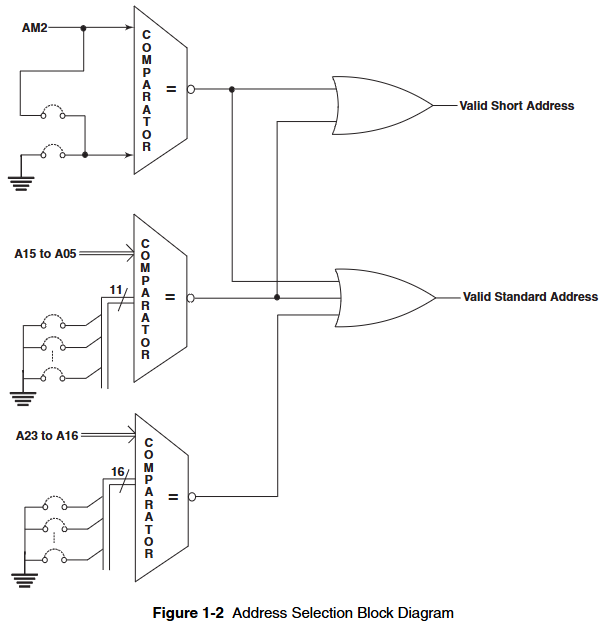
In register enabled mode, in addition to basic functions, it also includes registers in the short I/O space that involve multi host operations from the chassis.
Supports 8-bit, 16 bit, and 32-bit data transmission, and supports 16 bit, 24 bit, and 32-bit addressing.
The VMEbus system is completely electrically isolated from each other, with fiber optic cables up to 6560 feet (2000 meters) in length.
Compared to standard repeaters, the advantages include compact cables, strong noise resistance, high voltage isolation, and no electromagnetic interference from cables.
Slave repeaters include bus arbitrators, bus requesters, system controllers, and control/status registers, used to operate and monitor slave chassis in redundant repeater links or multi host applications.
Features
Overview
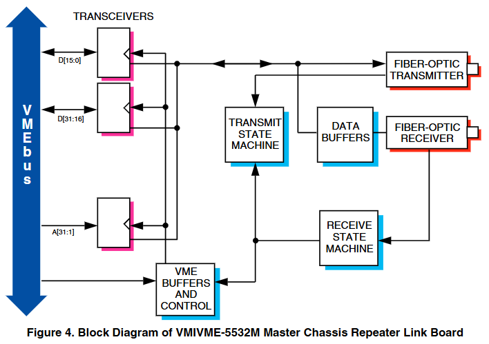
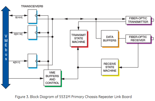
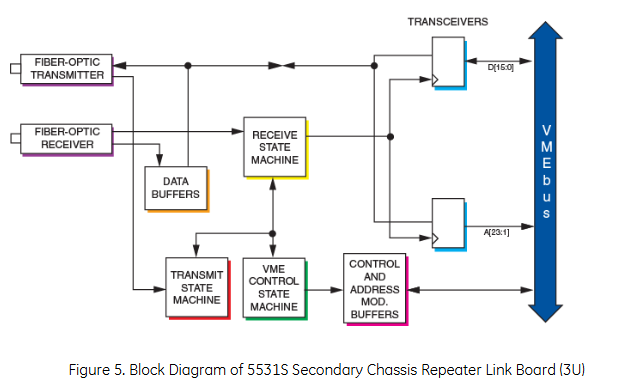
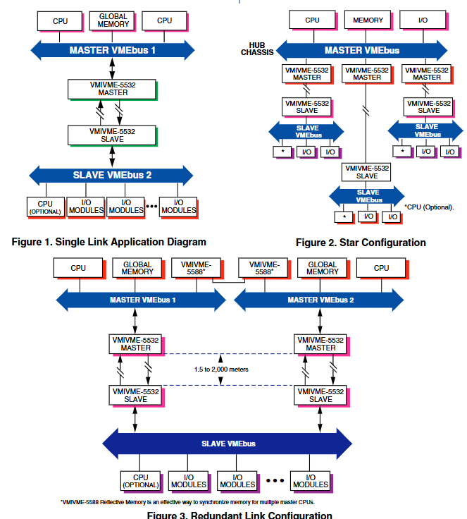
The master VMEbus chassis can communicate with multiple slave chassis by using multiple relay links in a star configuration. Any VMEbus host in the host chassis can access (read or write) any slave board in the slave chassis, and only non interrupt slave boards are allowed in the slave chassis. When a VMEbus host (usually a CPU board) addresses any card in the slave chassis, the link between the host chassis and the slave chassis is automatically established. Whenever a host in the main chassis issues a VMEbus read/write cycle, it will be repeated to the slave chassis. If any slave board in the slave chassis responds to the address, data transfer (read or write) will occur between the chassis and a data transfer acknowledgement (DTACK) will be generated to the host (in the main chassis) to complete the cycle.
VMEbus compatibility
Compliant with VMEbus specification revised version C1, supporting A32, A24, A16, as well as D32, D16, D08 (EO). Among them, VMIVME-5532M is a DTB slave (used for the main chassis), and VMIVME-5532S is a DTB master (used for the sub chassis), both with dual height and single slot external specifications.
Arbitrator and Requester
Arbitrator: SGL
Requester: ROR, only supports bus request level 3 (BR3 *)
BG3IN * – BG3OUT * Maximum latency: 100 ns
BG3IN * – BBUSY * Maximum latency: 200 ns
Link register (available when enabled)
Including board recognition, burst mode, host bus authorization, VMEbus activity (slave chassis), burst mode key, VMEbus key, Sysreset enable key, slave chassis reset key, etc.
Repeat to the VMEbus signal from the chassis
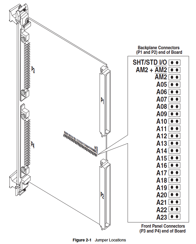
A1 to A31, D0 to D31、DS0*、DS1*、WRITE*、SYSRESET*、SYSCLK、AM0、AM2、AM4、AM5、LWORD* And IACK * (note: the following signals are regenerated from the chassis rather than sent through fiber optic cables: SYSCLK, AM0, AM1, AM3, and IACK *).
Return the VMEbus signal to the host box
D0 to D31, DTACK*
Active but non repetitive VMEbus signals from the chassis
BR0*-BR3*、BGIN0*-BGIN3*、BG0OUT*-BG3OUT*、BBSY*
Other parameters
Address modifier: 09, 0D, 29, 2D, 39, 3D
Read cycle overhead: maximum 4.0 µ s
Write cycle cost: maximum 4.0 µ s
Transmission rate (maximum) (10 foot cable length): Assuming the slave board in the chassis responds within 250 ns, with a minimum of 1MB/s (D32)
Cable specifications
Mode: Multi mode
Length: 5 to 6560 feet (1.5 to 2000 meters)
Fiber size: 62.5 microns
Package size: 125 microns
Buffer layer size: 900 microns
Maximum attenuation at 1300nm (including connector): 9.0 dB
Bandwidth at 1300nm: 500 MHz km
Protective cover length: 20 to 60 mm
U. L./NEC rating: OFNP
Connector style: ST, 2.5mm bayonet, both ends
Quantity required for each link: 2 (cables that meet this specification are provided with VMIVME-5532L. If you need to order cables separately, please refer to specification number VMICBL-000-F3-XXX)
Physical/Environmental Specifications
Size: Double height (6U) board 160 × 233.35 mm
Power requirements: VMIVME-5532S is a typical 2A at 5 VDC, with a maximum of 2.5 A; VMIVME-5532M is a typical 2A at 5 VDC, with a maximum of 2.5 A
Temperature: Operating temperature 0 to 65 ° C, storage temperature -20 to 85 ° C
Humidity: Relative humidity during operation is 20% to 80%, with no condensation
Altitude: up to 10000 feet (3048 meters) during operation
Cooling: forced air convection
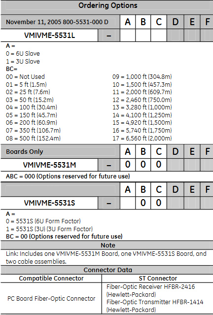
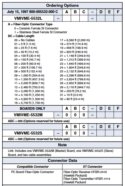
Ordering Options
In VMIVME-5532L, A represents the type of fiber optic connector (0=ceramic core ST connector, 1=stainless steel core ST connector), and BC represents the cable length (00=no cable, 01=5 feet (1.5 m) and other options).
Only the VMIVME-5532M and VMIVMME-5532S cards have corresponding ordering options, with ABC of 000 (options reserved for future use).
The link includes one VMIVME-5532M (master) board, one VMIVME-5532S (slave) board, and two cable assemblies.
Connector data
Compatible connector: ST connector
Printed Circuit Board Fiber Optic Connectors: Fiber Optic Receiver HFBR-2416 (HP), Fiber Optic Transmitter HFBR-1414 (HP)