Call us 24/7uaedcs@163.com
Welcome to the official website of CNIACS Automation Technology Co., Ltd!
Call us 24/7uaedcs@163.com

TEKTRONIX 4K/UHD Monitoring and Measurement Guidelines

Background and 4K/UHD basic specifications

Tektronix’s “4K/UHD Content Creation Guide” aims to address the technical pain points throughout the entire process of 4K/UHD content acquisition, storage, post production, and transmission. The core focus is on “how to ensure signal compliance and content quality through professional monitoring tools”, and it is recommended to use Tektronix 8000 series waveform monitors/rasterizers as the core equipment.

4K/UHD core specifications

Category Details Key Parameters

Resolution movie level 4096 × 2160 pixels

Home grade (UHDTV1) 3840 × 2160 pixels

Enhanced technology with dynamic range support for HDR (high dynamic range) to enhance light and dark details

Color gamut supports ITU-R BT.2020 wide color gamut (wider coverage than BT.709)

Signal transmission high frame rate (50p/59.94p/60p) four link 3G-SDI

Low frame rate (23.98p-30p) HD-SDI

6 Core Challenges in 4K/UHD Content Creation

Challenge 1: Inter channel timing synchronization of Quad Link signals

The four link 4K/UHD signal consists of four independent SDI physical links. Due to differences in transmission paths (cable length, equipment delay), timing deviations are prone to occur, resulting in signal splicing errors.

Standard requirements:

According to SMPTE ST 425-5 standard, the inter channel delay at the output end of the device should be ≤ 400ns (approximately 29 clock cycles);

There is no unified standard for the receiving end, and users need to control the delay difference themselves. Tek 8000 series devices can tolerate a maximum of 1024 clock differences.

Monitoring and investigation:

Using Tek 8000 series patented Timing Display, compare the horizontal/vertical offset of Link B/C/D with Link A as a reference;

If a “Video Format Mismatch” error occurs, switch to “Single Link” mode and check if the formats (resolution, frame rate) of each link are consistent;

Check the specific delay value through “MEAS>Timing Display” and adjust the transmission path (such as replacing equal length cables).

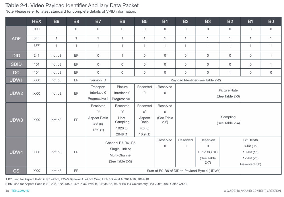
Challenge 2: Video Payload Identifier (VPID) Monitoring

VPID (based on SMPTE ST 352 standard) is stored in the auxiliary data area for devices to quickly identify video formats (resolution, sampling rate, number of links, etc.), and is key to 4K/UHD format compatibility.

VPID structure and key fields:

VPID data consists of 5 core components: Ancillary Data Flag(ADF)、Data Identifier(DID=41h)、Secondary Data Identifier(SDID=01h)、 4 user data words (UDW1-4), checksum (CS), where:

Example of UDW Byte Core Function Key Values

UDW1 identification standard and link type 89h=SMPTE ST 425-5 (four link 3G-SDI), C0h=ST 2081-10 (single link 6G-SDI)

UDW2 image frame rate 2h=24/1.001fps, 5h=25fps, Ah=60/1.001fps

UDW3 sampling rate and color gamut 0h=4:2:2 (YCbCr), 2h=4:4:4 (RGB); 0h=BT.709、2h=BT.2020

UDW4 link number 01h=Link A, 41h=Link B, 81h=Link C, C1h=Link D

Monitoring tools and troubleshooting:

Video Session Display: Directly view the UDW1-4 bytes of each link’s VPID. Normal four links require UDW1-3 to be consistent, and UDW4 should be 01h/41h/81h/C1h in the order of A → D;

ANC Data Inspector: locates the field/line position of VPID packets (such as Field1/Line9), verifies the checksum (Exp/ACT Chksum must be consistent);

Common problem: Link sequence error (such as Link B/C switching), physical connection needs to be adjusted to make UDW4 conform to the order.

Challenge 3: Choosing the right color gamut

4K/UHD supports ITU-R BT.709 (traditional HD color gamut) and ITU-R BT.2020 (wide color gamut). Choosing the wrong color gamut can result in color distortion, which needs to be matched with content requirements and display devices.

Two major color gamut core differences (CIE 1931 coordinates):

|Color gamut standard | Red (x, y) | Green (x, y) | Blue (x, y) | Applicable scenarios|

|ITU-R BT.709 | (0.640, 0.330) | (0.300, 0.600) | (0.150, 0.060) | Traditional HD, 4K compatible HD content|

|ITU-R BT.2020 | (0.708, 0.292) | (0.170, 0.797) | (0.131, 0.046) | 4K wide color gamut content (such as HDR videos)|

Color gamut conversion and verification:

The difference between brightness (Y) and color difference (Pb/Pr) calculation: The Y formula for BT.2020 is Y=0.2627R ‘+0.6780G’+0.0593B ‘, and BT.709 is Y=0.2126R’+0.7152G ‘+0.0722B’;

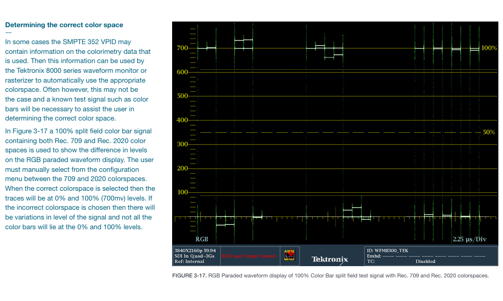
Verification method: Using 100% split field color bar signals (including BT.709 and BT.2020 dual color gamut), in RGB waveform display, the signal level should be stable at 0% (0mV) and 100% (700mV) under the correct color gamut, without significant fluctuations.

Challenge 4: Determine the aspect ratio of input 4K/UHD content

The aspect ratio of 4K/UHD content varies depending on the application scenario (movies, TV), and it is necessary to verify whether the image is scanned and cropped correctly to avoid stretching or cropping.

Common aspect ratios and corresponding resolutions:

|Aspect ratio | Application scenarios | Image size (pixels) | Effective pixels/line|

|16:9 (1.778:1) | UHDTV1 (Home) | 3840 × 2160 | 3840 pixels/2160 rows|

|1.896:1 | 4K Movie (Standard) | 4096 × 2160 | 4096 pixels/2160 lines|

|1.85:1 | widescreen movie | 3996 × 2160 | 3996 pixels/2160 lines (first line 83, last line 2242)|

|2.39:1 | Ultra widescreen movie | 4096 × 1716 | 4096 pixels/1716 lines|

Verification steps:

Vertical direction: Use the “Line Select” mode to check the effective signals of the first row (such as row 83 corresponding to 1.85:1) and the last row (row 2242);

Horizontal direction: Display with “Datalist”, check the first pixel (such as sample 50 corresponding to 1.85:1) and the last pixel (sample 4045) to ensure that the image is not cropped.

Challenge 5: Meet the high-quality requirements of 4K/UHD content

4K/UHD viewers have higher expectations for image quality and need to monitor brightness, color gamut, audio volume, etc. through strict quality control (QC) to ensure compliance and not disrupt artistic intent.

Core monitoring dimensions of QC:

|Monitoring Type | Standard/Threshold | Tool Configuration|

|Video color gamut | RGB color gamut: Set diamond area threshold (such as 1% deviation alarm); Brightness: -230mV~120IRE | Tek 8000 series “Gamut Thresholds” menu, supports EBU-R103 preset|

|Audio loudness | Compliant with EBU R128 (target -23 LKFS), ITU-R BS.1770 | “Loudness Settings” menu, set alarm threshold (such as ± 2 LU deviation)|

|Signal error | Freeze frame, black field detection, SDI link error | “Alarms” menu, enable screen prompts, logging, and beep alarms|

Error recording and tracing:

Record error types (such as “RGB Gamut Error”) in the associated timecode (e.g. 00:08:16:02);

The error log can be downloaded as a file and sent to the post production team along with the content to quickly locate the problem frame.

Challenge 6: Selection of Transmission Methods for 4K/UHD Signals

The four link signal needs to go through the “splitting transmission reassembly” process, with two mainstream splitting modes that match the transmission protocol supported by the device.

Comparison of two transmission modes:

|Transmission mode | Split logic | Advantages | Applicable scenarios|

|Square Division | Divide 4K images into 4 quadrants (Link A=upper left, B=upper right, C=lower left, D=lower right), each quadrant packaged as an independent SDI | Simple logic, easy to reorganize | Post production equipment (such as editing machines, color palettes)|

|Two Sample Interleave | Split by horizontal pixel groups: every 2 adjacent pixels are grouped and allocated to 4 links (such as pixel 0/4/8 → Link A, 1/5/9 → Link B) | Low memory usage, high transmission efficiency | Signal transmission links (such as broadcasting networks, satellite transmission)|

Mode configuration and validation:

Tek 8000 series: automatically recognizes VPID and standard recognition mode, or manually selects “Tile” or “Sample Interleaved” in “CONFIG MENU>Quad SDI Mode”;

Verification: Confirm through image display (Rasterizer) that there is no misalignment after recombination (such as no black edges, no pixel offset).

image.png

Recommended monitoring tools and reference resources

1. Tektronix core equipment

Equipment series types, core functions, applicable scenarios

WFM8000 waveform monitor for high-precision measurement (timing, color gamut, VPID), supporting four link synchronous monitoring signal acquisition, engineering testing, and main control room

WVR8000 waveform grating instrument image display+waveform monitoring, supporting 4K/UHDTV1, including quality alarm content creation (post production, color grading), and content distribution

2. Reference standards and resources

Timing: SMPTE ST 425-5 (four link timing) SMPTE ST 352(VPID);

Color gamut: ITU-R BT.709, ITU-R BT.2020;

Loudness: EBU R128, ITU-R BS.1770;

Key issues

Question 1: How to troubleshoot channel timing deviation issues using Tektronix 8000 series devices in four link 4K/UHD signal transmission? Please refer to the standard requirements and operating procedure instructions.

Answer: Four link timing deviation needs to be checked according to SMPTE ST 425-5 standard (device output delay ≤ 400ns). The Tek 8000 series operation steps are as follows:

Preliminary check for link format consistency:

If the status bar displays “Video Format Mismatch”, switch to “Single Link” mode, open the “Video Session” display, confirm that the resolution (such as 3840 × 2160), frame rate (such as 59.94p), and sampling rate (such as 4:2:2) of Link A/B/C/D are completely consistent, and eliminate timing misjudgments caused by format differences;

Enable Timing Display to monitor latency:

Go to “MEAS>Timing Display” and use Link A as a reference (default) to check the “Horizontal Offset” and “Vertical Offset” of Link B/C/D relative to Link A. The Tek 8000 series can tolerate a maximum clock difference of 1024, and if exceeded, it cannot be correctly spliced;

Adjust transmission path:

If the delay of a certain link exceeds the standard, priority should be given to checking the cable length (replacing equal length 3G-SDI cables), followed by investigating the delay differences of intermediate devices (such as switches and distributors), adjusting and re monitoring until the delay of all links is ≤ 400ns;

External reference calibration (optional):

If higher accuracy is required, a black field or three-level reference signal can be connected to the “External Reference” port of the instrument to compare the timing of Link A with the reference signal and further calibrate the link delay.

Question 2: What is the role of VPID (Video Payload Identifier) in 4K/UHD systems? How to verify the correctness of VPID through Tek 8000 series devices, and what are the common errors?

Answer: VPID is based on the SMPTE ST 352 standard and stored in the SDI auxiliary data area. Its core function is to enable devices to quickly recognize video formats (resolution, number of links, sampling rate, color gamut, etc.), avoiding manual configuration errors. It is a “format passport” compatible with multiple 4K/UHD devices.

1、 Steps to verify VPID for Tek 8000 series:

Quick verification of video sessions:

Open the “Video Session” display (Page 1) and view the “352M Payload” field (i.e. UDW1-4 bytes of VPID) for each link:

The four links must meet the following requirements: UDW1-3 (format information) is completely consistent (such as 89h CAh 00h), UDW4 (link number) is 01h → 41h → 81h → C1h according to A → D;

ANC Data Inspector deep validation:

Go to “ANC Data Inspector”, filter for “DID/SDID=41/01” (VPID identification), and view:

Checksum (Exp/ACT Chksum): must be consistent, otherwise VPID data will be damaged;

Location information: Normal VPID is located at “Field1/Line9”, abnormal location may cause the device to not recognize it;

Datalist locates sample level information:

Based on the “Line” and “Sample” displayed by the ANC Inspector, locate the VPID packet in the “Datalist” and confirm that UDW1-4 bytes have no bit errors (such as stuck bits).

2、 Common VPID errors and reasons:

Link number error: UDW4 is not in the order of A → D (01h/41h/81h/C1h), such as Link B/C exchange, resulting in device splicing image misalignment;

VPID duplication/missing: If there are multiple VPIDs on the same link or if a link does not have a VPID, the device cannot determine the format, resulting in an “unknown format” error message;

Checksum mismatch: Data is damaged during signal transmission, and cable shielding needs to be checked or intermediate equipment (such as SDI distributor) needs to be replaced.

Question 3: How to choose between BT.709 and BT.2020 color gamut in K/UHD content creation? How to verify the correctness of color gamut settings through testing signals with Tek 8000 series devices?

Answer: Color gamut selection needs to be combined with content usage and display device capabilities, and verification relies on standard test signals and professional monitoring tools, as follows:

1、 Color gamut selection principle:

Choose the scene for BT.709:

The content needs to be compatible with traditional HD devices (such as old TVs and HD players);

The production environment does not have BT.2020 display devices (such as the monitor only supporting BT.709) to avoid color deviation in the later stage;

Choose the scene for BT.2020:

4K HDR content (such as movies and high-end TV programs) needs to utilize a wide color gamut to enhance color richness;

The target display device supports BT.2020 (such as 4K HDR TV, professional cinema projection).

2、 Color gamut correctness verification steps (using Tek 8000 series):

Prepare test signal:

Generate a “100% split color bar signal” (left half BT.709, right half BT.2020), ensuring that the signal contains RGB three channel full range levels (0% -100%);

Switching instrument color gamut settings:

Go to “CONFIG MENU>Colorimetry”, select “BT.709” and “BT.2020” respectively, and observe the RGB waveform display:

Correct setting: The RGB level of the corresponding half is stable at 0% (0mV) and 100% (700mV) without fluctuations;

Error setting: The RGB level of non corresponding half deviates by 0%/100% (for example, under BT.709 setting, the green level of BT.2020 half is only 80%);

Comparison brightness and color difference formula:

Go to “MEAS>Amplitude>Y” and measure the brightness value:

BT.709:Y=0.2126R’+0.7152G’+0.0722B’, The Y value of the white color bar is approximately 700mV;

BT.2020:Y=0.2627R’+0.6780G’+0.0593B’, The Y value of the white color bar is approximately 680mV;

If the values match, the color gamut setting is correct, and if the deviation exceeds 5%, it needs to be readjusted.

Tektronix 5 Series Mixed Signal Oscilloscope (MSO54/56/58)

Core parameters and characteristics of the product

1. Basic hardware specifications

Category detailed parameters

Channel configurations MSO54 (4 channels), MSO56 (6 channels), and MSO58 (8 channels) all support FlexChannel technology, and a single channel is compatible with:

-Analog probe (TekVPI) ®  Or BNC interface)

-8-channel digital probe (TLP058 FlexChannel Logic Probe)

Bandwidth range: Basic bandwidth of 350 MHz (default), supports upgrades: 500 MHz, 1 GHz, 2 GHz (requires corresponding bandwidth options, such as SUP5-BW3T54)

Sampling performance with a maximum sampling rate of 6.25 GS/s, supporting real-time sampling, interpolation real-time sampling, and equivalent time sampling (only applicable to repetitive signals)

Record length standard 62.5 M points/channel, optional upgrade to 125 M points/channel (options 5-RL-125M/SUP5-RL-125M)

15.6-inch HD capacitive touch screen (1920 × 1080 pixels) with optimized touch operation logic, supporting multi finger gestures, double-click configuration, etc

Capture capability up to 500000 waveforms per second, FastAcq mode can reduce waveform acquisition dead time and accurately capture transient events such as spikes and short pulses

Optional integrated functions include a 50 MHz arbitrary function generator (AFG), digital multimeter (DVM), and trigger frequency counter

2. Core technological advantages

FlexChannel technology: No need to replace hardware modules, single channel can switch between analog/digital signal acquisition, flexible adaptation to mixed signal debugging scenarios.

Multidimensional triggering system: covering basic triggering, advanced triggering, and bus triggering, it can accurately capture target signal events.

Unrestricted waveform display: Supports unlimited display of mathematical waveforms, reference waveforms, and bus waveforms (limited by system memory).

TekSecure security feature: supports secure memory erasure and protects sensitive test data.

Accessories and optional features

1. Standard accessories (included with the box)

Accessory Name Quantity Specification/Purpose Tektronix Model

Installation and Safety Manual 1 Instrument Installation and Safety Operation Guide 071-3514-xx

Passive voltage probe, one 350/500 MHz model per channel, equipped with TPP0500B (500 MHz bandwidth); 1/2 GHz model with TPP1000 (1 GHz bandwidth) TPP0500B, TPP1000

Front panel cover 1 protects the instrument front panel interface 200-5406-xx

Accessory bag 1 stores small accessories, attached to the front panel cover 016-2106-xx

Wired USB Mouse 1 Auxiliary Operation Interface 119-7054-xx

The voltage standard for power cord 1 to adapt to the corresponding region depends on the region

Calibration Certificate 1: Instrument Factory Calibration Certificate N/A

2. Recommended accessories (optional)

Accessory name, purpose, model/specification

Hard transport box instrument transportation protection HC5

Rack installation kit installs the instrument onto a standard equipment rack (requiring 7U space) RM5

Mini keyboard for convenient text/parameter input 119-7275-xx

GPIB-USB adapter implements GPIB interface extension TEK-USB-488

TekVPI to BNC adapter compatible with BNC probe and TekVPI interface TPA-BNC

Off ramp pulse generator assisted multi-channel off ramp calibration 067-1686-xx

High voltage differential probe for high voltage signal measurement (such as THDP0100: ± 6 kV, 100 MHz) THDP0100, THDP0200, etc

Current probe current signal measurement (such as TCP0020: 50 MHz, 20 A AC/DC) TCP0020, TCP0030A, etc

3. Core optional function options

Function Category Options Model Details Features

Arbitrary Function Generator (AFG) 5-AFG (pre installed), SUP5-AFG (upgraded) – waveform types: sine, square wave, pulse, ramp, etc. 13 preset waveforms+arbitrary waveform

-Maximum frequency: 50 MHz (sine wave)

-Maximum output amplitude: 5 Vp-p (high impedance load)

-Sampling rate: 250 MS/s, any waveform recording length of 128K samples

Advanced Jitter Analysis (DJA) 5-DJA (pre installed), SUP5-DJA (upgraded) – supports 30+industry standard jitter and eye chart measurements: TIE TJ@BER 、 DDJ、DCD、 Eye height, eye width, Q factor, etc

-Generate analysis views such as jitter summary table, bathtub curve, eye diagram, etc

Bandwidth upgrade SUP5-BW3T54 (4-channel 350 → 500 MHz), SUP5-BW3T104 (4-channel 350 → 1 GHz), SUP5-BW3T204 (4-channel 350 → 2 GHz), etc. – Partial upgrades only require a license (such as 350 → 500 MHz), while high bandwidth upgrades need to be sent back to the service center for hardware replacement

-Upgrade with calibration data and new front-end bandwidth labels

Serial bus triggering and analysis -5-SRAUDIO (audio bus), 5-SRAUTO (car bus), 5-SRCOMP (computer bus), 5-SRENET (Ethernet), 5-SREMBD (embedded bus), 5-SRUSB2 (USB 2.0) – supports buses: I2S, LJ, RJ, TDM (audio); CAN, LIN, FlexRay (automotive); RS-232/422/485/UART (computer); 10BASE-T/100BASE-T (Ethernet); I2C, SPI (embedded); USB 2.0 LS/FS/HS

Record length upgrade 5-RL-125M (pre installed), SUP5-RL-125M (upgraded) will increase the default 62.5M point/channel record length to 125M point/channel, which can capture more waveform data points

Service options T3 (3-year warranty), T5 (5-year warranty), C3 (3-year calibration), C5 (5-year calibration) – warranty includes parts, labor, and domestic transportation within 2 days

-Calibration includes traceable verification reports, covering initial calibration and subsequent annual calibration

Instrument installation and basic configuration

1. Preparation before installation and environmental requirements

(1) Accessory inspection

After unpacking, it is necessary to verify all items against the packing list, including the host, standard accessories, and selected option modules/probes, to confirm that there are no missing or damaged items.

(2) Environmental and power requirements

Category requirements details

The working temperature is 0 ° C~+50 ° C (+32 ° F~+122 ° F), and at least 2 inches (51 mm) of ventilation space should be reserved on both sides and the rear of the instrument

Working humidity 5%~90% relative humidity (≤ 40 ° C); 5%~55% relative humidity (>40 ° C~50 ° C), no condensation

Working altitude up to 3000 meters (9842 feet)

Power specification voltage: 100 V~240 V AC RMS (± 10%), single-phase

Frequency: 50/60 Hz (90 V~264 V), 400 Hz (103 V~127 V)

Maximum power consumption: 400 W (all models)

2. Key configuration steps

(1) Probe connection and compensation

Probe compensation is the core step to ensure measurement accuracy. Taking the TPP0500B/TPP1000 passive probe as an example:

Connect probe: Insert the probe into the FlexChannel connector and hear a “click” sound to indicate it is locked in place. The TekVPI probe will automatically configure channel parameters (bandwidth, attenuation, etc.).

Connect compensation signal: Connect the probe tip to the 1 kHz square wave source (lower terminal) of the instrument front panel “PROBE COMP”, connect the probe ground clamp to the ground terminal (upper terminal), and remove the probe tip accessory to ensure good contact.

Display Square Wave: Press the “Autoset” button on the front panel, and the screen will display a stable 1 kHz square wave.

Perform compensation: double-click the channel badge (such as Ch1) → open the “Probe Setup” panel → click on “Compensate Probe”, wait for compensation to complete, and the status bar will display “Pass” to indicate success (if “Fail” is displayed, the probe needs to be reconnected and the operation repeated).

(2) Signal Path Compensation (SPC)

SPC is used to correct DC deviations in internal signal paths caused by temperature changes or long-term drift. It is recommended to:

Execute when the ambient temperature changes by more than 5 ° C (41 ° F);

Execute once a week (if the commonly used vertical scale is ≤ 5 mV/div).

Operation steps:

Disconnect all probes, cables, and external signal inputs;

Preheat the instrument for at least 20 minutes when powered on;

Select “Utility>Calibration>Run SPC” from the top menu bar;

Wait for the compensation to be completed (several minutes per channel), and the status bar will display “SPC Pass”. If it fails, record the error message and contact the support team.

(3) Network and Remote Access Configuration

Physical connection: Connect the instrument LAN port to the network switch/router using CAT5 Ethernet cable;

Network settings:

Select “Utility>I/O>LAN”;

Automatic IP acquisition (default): Select “Auto”, and the instrument obtains the IP address, subnet mask, and gateway through DHCP;

Manual settings: Select “Manual” and enter the static IP, subnet mask, and DNS address provided by the IT department;

Connection verification: Click on “Test Connection”, the LAN status icon turns green to indicate successful connection;

Remote access: Enter the instrument IP address in a PC browser on the same network and select “Instrument Control (e * Scope ®)”, The instrument can be remotely operated through a browser (supporting mouse control of all interface functions).

(4) Channel skew (Desk view)

When measuring multi-channel timing, it is necessary to correct the propagation delay difference between probes, and two methods are supported:

Quick visual method:

Connect all probes to the “PROBE COMP” signal and activate the corresponding channel;

Double click on the waveform view and set “Waveform Mode” to “Overlay”;

Adjust the horizontal scale to clearly display channel delay differences;

Double click on the target channel badge ->”Other” ->”Deskew”, adjust with the multifunction knob to align the waveform edge with the reference channel.

Measurement method:

Add “Delay” measurement (“Add New… Measure>Timing>Delay”);

Set the reference channel as Source 1 and the target channel as Source 2;

Adjust the Desk value of the target channel to minimize measurement delay.

Detailed explanation of core operations and functions

1. Signal acquisition and triggering system

(1) Fast waveform display (Autoset)

Press the “Autoset” button on the front panel, and the instrument will automatically complete the following operations:

Analyze the signal characteristics of the lowest numbered display channel (analog/digital);

Adjust horizontal (time base), vertical (scale, position), and trigger parameters;

Stable display waveform (optimizing the vertical scale of all active waveforms in stacking mode and evenly distributing waveforms in stacking mode).

Note: AutoSet ignores mathematics, reference, and bus waveforms, and signals with frequencies<40 Hz will be judged as “no signal”.

(2) Collection mode selection

By double clicking the “Acquisition” badge, the following modes can be selected:

Applicable scenario characteristics of the mode

Sample: Conventional signal acquisition retains the first sample of each acquisition interval without post-processing

Peak Detection captures high-frequency spikes and alternates between narrow pulses to preserve the highest/lowest samples of adjacent acquisition intervals

High Res high-precision measurement, low-noise scene based on sampling rate FIR filtering, suppresses aliasing, ensures ≥ 12 bit vertical resolution, supports FastAcq

Envelope observes the range of signal changes, captures the extreme values of multiple collected signals, and displays the envelope waveform

Average reduces the average waveform of random noise collected multiple times, and the average frequency can be set

FastAcq captures transient events to reduce acquisition dead time, supports intensity display (reflecting signal frequency), and can choose color palettes such as “Temperature” and “Spectral”

(3) Trigger type and configuration

Trigger is used to define when to start collecting waveforms. The 5 series supports a variety of trigger types, including:

Edge trigger (basic):

Trigger source: any analog/digital channel, mathematical/reference waveform;

Slope: rising edge, falling edge, arbitrary edge;

Level: Double click the “Level” knob to set it, or press the knob to automatically set it to 50% of the signal peak to peak value;

Coupling: DC (transmitting all signals), HF Reject (attenuation>50 kHz signals), LF Reject (attenuation<50 kHz signals), Noise Reject (increasing hysteresis, anti noise).

Pulse width trigger:

Trigger conditions: Pulse width<,>,=, ≠ set value, or within/outside the specified range;

Polarity: positive pulse, negative pulse, any polarity;

Application scenario: Narrow pulse and wide pulse fault detection in digital logic.

Bus trigger:

Prerequisite: Corresponding buses (such as CAN, I2C) have been added;

Configuration steps:

Click on “Add New Bus” → select the bus type (such as CAN);

Set bus parameters (such as CAN baud rate, signal source, threshold);

Double click the “Trigger” badge ->select “Trigger Type>Bus” ->select the trigger bus (such as Bus1);

Set triggering conditions (such as CAN ID, data bytes, frame type).

Timing trigger (A&B events):

Function: After triggering event A, data collection will only be initiated upon detecting event B;

to configure:

Select ‘Trigger Type>Sequence’;

Configure event A (such as Ch1 rising edge);

Configure event B (such as Ch2 pulse width>100 ns);

Set trigger logic: trigger the first B event (with a delay time that can be set), or the Nth B event.

2. Measurement and analysis functions

(1) Basic measurement operation

Add measurement: Click on “Add New… Measure” in the results bar ->select the measurement source (such as Ch1) ->select the measurement category (amplitude, timing, jitter, etc.) ->double-click the measurement item (such as “Peak to Peak”), and the measurement badge will be automatically added to the results bar.

Measurement configuration: Double click the measurement badge → Open the configuration menu, you can:

Label (for easy identification, such as “VCC peak to peak value”);

Set reference level (such as 10% -90% rise time threshold);

Enable statistical display (mean, minimum, maximum, sample size);

Set measurement gating (only measure specific areas of the waveform, such as between the cursor and the screen display area).

(2) Core measurement categories and parameters

Application scenarios of key measurement items in measurement categories

Peak to peak value, maximum value, minimum value of amplitude measurement AC RMS、DC、 Analysis of positive/negative overshoot, top, bottom, and area voltage/amplitude characteristics (such as power ripple, signal amplitude consistency)

Timing measurement of frequency, cycle, rise/fall time, pulse width, duty cycle, delay, phase, data rate, and verification of unit interval signal timing characteristics (such as clock frequency, signal delay, duty cycle deviation)

Jitter measurement (basic) time interval error (TIE) preliminary jitter detection

Jitter Measurement (Advanced, requires DJA option) Deterministic Jitter (DJ), Random Jitter (RJ), Total Jitter( TJ@BER )Data related jitter (DDJ), periodic jitter (PJ), high-speed serial signal (such as USB, Ethernet) jitter compliance testing

Eye diagram measurement (DJA option required) eye height, eye width, eye height @ BER, eye width @ BER, Q-factor high-speed signal integrity assessment (such as SerDes, DDR)

(3) Bus decoding and analysis

Taking CAN bus as an example (requires 5-SRAUTO/SUP5-AFG options):

Add CAN bus:

Click on “Add New Bus” → select “Bus Type>CAN”;

Set “Source” (channel connected to CAN_SH), “Threshold” (logic high level, such as 1.4 V), “Bit Rate” (such as 500 kbps), and “Identifier Format” (standard 11 bits/extended 29 bits);

Decoding display: The bus waveform is automatically displayed, and the decoding result is superimposed on the waveform (such as ID=0x123, Data=0x01 0x02);

Add bus result table: Click on the results bar “Results Table>Bus Decoder” to generate a table containing ID, data, frame type, and timestamp, which can be saved as a. csv file.

(4) Waveform Analysis View

In addition to conventional waveform display, it supports multiple analysis views:

Histogram: Display the distribution of measurement values (such as amplitude distribution, jitter distribution), double-click the measurement badge → click “Histogram” to add;

Spectrum: Display the frequency components of the signal. Double click the measurement badge ->click “Spectrum” to set the FFT window (rectangle, Hanning, Hamming, etc.);

Eye Diagram: To select the DJA option, double-click on the jitter measurement badge and then click on “Eye Diagram” to configure the eye diagram template and BER threshold;

Time Trend: Display the change of measurement values over time (such as long-term drift of power supply voltage), double-click the measurement badge → click “Time Trend”.

3. Display and operation optimization

(1) Waveform display mode

Stacking mode (default): Each waveform is vertically stacked in independent “slices”, with independent vertical scales for easy observation of multi-channel signals;

Overlay mode: All waveforms are stacked in the same grid for easy comparison of waveform shapes (such as reference waveforms and measured waveforms);

Switching method: Double click on the blank area of the waveform view ->click on “Display Mode” to switch.

(2) Zoom and cursor operation

Zoom mode enabled:

Press the “Zoom” button on the front panel;

Click on the “Draw-a-Box” in the results bar, drag and draw the area of interest on the waveform (automatically enters zoom mode);

Double click the “Zoom” icon in the upper right corner of the waveform view.

Zoom operation:

Zoom knob (middle): Adjust the size of the zoom box (zoom in/out);

Translation knob (outer side): Move the zoom box position (left and right translation);

Cursor measurement:

Press the “Cursors” button on the front panel, or click on “Add New… Cursors” in the results bar;

Use the multifunctional knobs A/B to move the cursor, supporting waveform cursor (measuring amplitude+time), vertical cursor (measuring time difference), and horizontal cursor (measuring amplitude difference);

Double click cursor reading → configurable cursor type and source (supports cross channel comparison).

4. Data storage and recall

(1) Can store data types and formats

Data Type Storage Format Usage

Screenshot in PNG, BMP, JPG format to save the current interface (including menu, waveform, measurement results) for document reporting

Waveform data. wfm (Tektronix specific),. csv (universal format) to save channel, mathematical, and reference waveform data for subsequent analysis or sharing

Instrument settings. set saves all channel, trigger, measurement, and display settings for easy repetition of testing scenarios

Report PDF, single file webpage containing measurement results, waveform screenshots, instrument configuration, annotations, supports adding custom notes

Conversation. tss (compressed file) saves settings and all waveform data for offline analysis or transfer of testing tasks

(2) Storage operation steps (taking saving waveforms as an example)

Select “File>Save As>Waveform”;

Configure storage parameters:

Save location: Select a USB drive (such as E:, F:) or internal storage (C:), click “Browse” to navigate to the folder;

File name: default “Tek000”, modifiable (supports Chinese/English), enable “Auto Increment File Name” to automatically increment numbers (such as Tek001, Tek002);

Save type: Choose. wfm (to preserve complete information) or. csv (to facilitate Excel analysis);

Save source: Select “All” (all active waveforms) or a single waveform (such as Ch1, Math1);

Click “OK” to save, and after successful saving, the status bar will display a confirmation message.

(3) Quick storage (User key)

First use: Press the “User” button on the front panel → open the “Save As” menu, configure the storage type (such as waveform), position, and format, and click “OK”;

Subsequent use: Press the “User” button again to automatically save data according to the previous configuration (no need to repeat the settings).

(4) Data recall operation (taking the recall reference waveform as an example)

Click on ‘Add New Ref’ (settings bar);

Select storage location (such as USB drive) and file type (. wfm);

Select the target waveform file, click “Recall”, and add the reference waveform (Rx) to the waveform view for comparative analysis.

Common problems and precautions

1. Safety precautions

ESD protection: When operating the probe or DUT, wear a grounded anti-static wristband (grounding terminal provided on the instrument front panel) to avoid touching the probe tip or instrument input interface;

Input voltage limit: When the analog channel is set to 1 M Ω, the maximum input is 300 VRMS, and when set to 50 Ω, the maximum input is 5 VRMS. Exceeding this limit may damage the instrument;

Power safety: Only use power cords that come with the box or are Tektronix certified, ensure good grounding, and avoid use in humid environments.

2. Common troubleshooting

Troubleshooting steps for fault phenomena

No waveform display. 1. Check if the probe connection is locked; 2. Confirm that the channel is enabled (click the “Inactive Channel” button in the settings bar); 3. Press the “Autoset” button; 4. Check if the trigger source is correct and if the trigger mode is “Auto”

Inaccurate measurement results: 1. Perform probe compensation; 2. Run SPC; 3. Check the reference level setting; 4. Confirm that there is no signal clipping (the channel badge displays “Clipping” and the vertical scale needs to be adjusted)

Network connection failure: 1. Check the network cable connection; 2. Confirm that the router/DHCP service is functioning properly; 3. Manually set static IP testing; 4. Restart the instrument and router

Option cannot be enabled. 1. Confirm that the license has been installed (“Help>About”); 2. Restart the oscilloscope; 3. Check if the license file corresponds to the instrument serial number

Tektronix TDS3000 series digital fluorescence oscilloscope

Basic Information

1. Product model and positioning

The TDS3000 series is a mid to high end digital fluorescence oscilloscope (DPO) launched by Tektronix, featuring high sampling rate and flexible analysis functions, covering multi scene signal debugging. The core models and parameters are shown in the table below:

Model Channel Number Bandwidth Maximum Sampling Rate Maximum Record Length Typical Application Scenarios

TDS3012B 2 100MHz 1GS/s 10k point basic analog signal debugging (such as audio)

TDS3014B 4 100MHz 1GS/s 10k point multi-channel low-speed signal (such as sensor)

TDS3032B 2 300MHz 2.5GS/s 100k point medium speed signal (such as 100Mbps communication)

TDS3034B 4 300MHz 2.5GS/s 100k point multi-channel medium speed signal (such as CAN bus)

TDS305232 500MHz 5GS/s 1M high-speed signal (such as 500MHz clock)

TDS3054B 4 500MHz 5GS/s 1M point multi-channel high-speed signal (such as PCIe)

2. Document and Service Support

Document scope: The manual covers device operation, functional applications, troubleshooting, and is applicable to firmware versions V4.XX and above;

Technical support: Call 1-800-833-9200 in North America, and visit the Tektronix official website for local hotlines in other regions; Support online download of drivers, application notes, and firmware updates;

Warranty Policy: The oscilloscope host comes with a 2-year warranty, and the probe (such as P6139A) comes with a 1-year warranty, excluding malfunctions caused by human damage or unauthorized repairs.

Basic Operation Guide

1. Device initialization and probe settings

(1) Power on and self-test

After turning on, the oscilloscope automatically performs a self-test. If it displays “PASS”, it is normal; If “FAIL”, check the power connection or contact for repair;

Press the Default Setup button to quickly reset to factory settings (vertical coupling DC, trigger edge rise, time base 200ns/grid).

(2) Probe connection and compensation

Probe selection: It is recommended to use Tektronix specialized probes, such as P6139A (100MHz/10X) and P6249 (500MHz/10X);

Connection steps: ① Connect the BNC end of the probe to the oscilloscope channel, ② Connect the probe tip to the measured signal point, ③ Connect the reference wire to the circuit ground;

Manual compensation: ① Connect the probe to the “probe compensation” terminal (output 5V/1kHz square wave), ② Display the waveform according to AutoSet, ③ Rotate the probe compensation screw until the waveform is free of overshoot/undershoot (standard square wave);

Attenuation setting: Channel menu ->”Probe Attenuation” Set to 1X/10X, which should match the actual attenuation ratio of the probe (default 10X).

2. Core control system operation

(1) Vertical system

Coupling mode:

DC: AC/DC signal, suitable for DC bias signals (such as power supply voltage);

AC: Block DC components (attenuation<10Hz signal), suitable for AC signals (such as audio);

Grounding: Disconnect the input to determine the zero level position;

Vertical Scale: Range 2mV-10V/grid (1-2-5 sequence), adjustable through the “Vertical Scale” knob; Support “fine adjustment” mode (switch by knob), achieve non-standard stepping (such as 2.5mV/grid);

Channel control: Press the channel button (CH1/CH2, etc.) to turn on/off the channel, move the “vertical position” knob up and down to display the waveform, and support channel overlay display (press Display → “Overlay”).

(2) Horizontal system

Time base range: 5ns-50s/grid (1-2-5 sequence), corresponding to the following sampling rate relationship (taking TDS3052B as an example):

Time base setting sampling rate maximum measurable frequency (Nyquist frequency)

5ns-200ns 5GS/s 2.5GHz

400ns-1μs 2.5GS/s 1.25GHz

2μs-50s 1GS/s 500MHz

Sampling mode:

Real time sampling: suitable for high-frequency signals (≤ bandwidth), directly capturing signals;

Equivalent sampling: suitable for ultra-high frequency signals (>bandwidth), reconstructing waveforms through multiple samplings;

Window function: Press Horiz Menu → “Window” to open, define waveform segments and zoom in to view, support switching between main timing and window view.

(3) Trigger system

Trigger type:

Edge trigger: Based on the rising/falling edge of the signal, the source can be selected as CH1-CH4/Ext/Ext 5x/mains power; Coupling supports DC/AC/noise suppression (reducing false triggering of high-frequency noise);

Video trigger: Supports NTSC/PAL/SECAM standards, with synchronization methods including all fields/odd fields/even fields/specified number of lines (1-525 NTSC, 1-625 PAL);

Pulse triggering: triggered by pulse width (20ns-10s), with conditions of>,<,=, ≠, suitable for abnormal pulse detection (such as burrs);

Code triggering: triggered based on logical combinations of 2-4 channels (such as CH1=high, CH2=low), supporting TTL/CMOS levels;

Key operation: Press Set to 50% to automatically set the trigger level to the midpoint of the signal peak to peak; Press Force Trigger to ignore triggering conditions and force collection.

Advanced functional applications

1. Waveform analysis and measurement

(1) Wave Inspector function

Core function: Quickly navigate long recorded waveforms (such as 1M points), avoiding the tedious operation of traditional knobs;

Operation control:

Zoom knob: The inner ring enlarges clockwise and shrinks counterclockwise, supporting separate scaling of X/Y axes;

Translation knob: Move the outer ring left and right to locate the target area;

Marking function: Set the markers (A/B/C/D) according to the markers, and display the time/amplitude difference between the markers;

Example: When analyzing the waveform of a 1M point serial bus, locate a specific data frame by scaling, pan to view the related waveforms before and after, and mark the measurement frame interval.

(2) Measurement function

Automatic measurement: Supports 29 types, with a maximum of 4 displayed at once. The commonly used types are shown in the table below:

Measurement type definition accuracy range

The frequency is calculated based on the first cycle, with units of Hz kHz MHz ± (0.01%+1 count)

Absolute difference between peak to peak maximum and minimum peak values ± (1%+2mV)

The time for the waveform to rise from 10% amplitude to 90% amplitude ± (3%+10ps)

The phase difference between the rising edges of two channel signals, in units of ± (2 °+0.1 °)

Operation steps: Press Measure → “Select Measurement” → Select Source and Type → View Real time Updated Readings;

Statistical analysis: Press “Statistics” to display the average, maximum, minimum, and standard deviation of the measured values (based on 50-1000 sampling points).

(3) FFT frequency domain analysis

Function definition: Convert time-domain (YT) signals into frequency-domain spectra, supporting 1024-1M FFT points;

Window function selection:

Window function characteristics applicable scenarios

Hanning has good frequency resolution and average amplitude accuracy. Analysis of frequency components of periodic signals

Flattop has high amplitude accuracy (± 0.1%), and its frequency resolution is generally calibrated for amplitude calibration (such as signal source output)

Rectangular without attenuation, severe spectral leakage of pulse/instantaneous signals (such as lightning waves)

Operation steps: Press Math → “FFT” → Select signal source → Set window function → Adjust frequency domain scale (Hz/grid).

2. Serial bus triggering and decoding

Supports bus types: I2C, SPI, UART (RS-232/422/485), CAN, LIN;

Trigger settings (using I2C as an example):

Press Trigger Menu ->”Type” select “Bus” ->”Bus Type” select “I2C”;

Define SCLK (such as CH1), SDA (such as CH2), and set a threshold (midpoint of the waveform);

Set triggering conditions (such as address=0x50, direction=write), capture the target frame as Single;

Decoding display: Press Decode → “Enable” to overlay color labels on the time-domain waveform (address yellow, data blue, stop red); Support viewing of “event table” (displaying timestamps, types, and values), which can be exported as CSV.

3. Extreme testing and sequence acquisition

(1) Extreme testing

Function definition: Customize “templates” (such as standard waveform contours), use an oscilloscope to compare the collected waveform with the template in real-time, and mark areas that exceed the tolerance;

Application scenario: Batch production testing (such as whether the power output waveform meets the standard);

Operation steps: ① Collect standard waveforms, ② Press Limit Test → “Create Template” → Adjust tolerance (such as ± 5%), ③ Turn on “Test”, display “FAIL” and mark the red area when exceeding the tolerance.

(2) Sequence collection

Function definition: Divide long signals into multiple segments (up to 100 segments) for acquisition, with each segment recording a length that is independently set (such as 10k points/segment);

Advantages: Save memory and capture intermittent burst signals (such as pulses with a 1-second interval and a duration of 10 μ s);

Operation steps: Press Acquire → “Sequence” → Set the number of segments and each segment length → Enable acquisition, and after completion, you can view the waveform segment by segment.

Data management and peripheral connectivity

1. Data storage

storage medium

Built in memory: supports 10k-1M point waveform storage, can save 50 sets of settings (. SET files);

USB flash memory: Supports ≤ 32GB, saving formats include:

Image: BMP/JPG (resolution 800 × 600);

Waveform: CSV (including time and amplitude data), TXT (Tektronix proprietary format);

Settings: SET (can directly call up applications);

Save steps: Press Save/Recall → “Save” → Select type/medium/path → Press “Confirm”.

2. Peripheral connection

GPIB: Connect to PC through GPIB interface (optional module required) and use TekVISA software to achieve remote control (such as automatic testing scripts);

Ethernet: Supports LXI-C standard, connects to LAN through Ethernet cable, and accesses oscilloscope IP address through browser to achieve remote operation and data transmission;

Printer: Connect to a PictBridge compatible printer, print screen images directly by pressing Print, and support ink saving mode (white background);

PC connection: Connect the PC through a USB cable, install OpenChoice software, and achieve real-time waveform display and data export.

Safety and Maintenance

1. Safety regulations

Grounding requirements: A power cord with a grounding pin must be used, with a grounding resistance of ≤ 0.1 Ω to avoid electric shock;

Overvoltage protection: The maximum voltage of the input channel is ≤± 400V (DC+AC peak). If it exceeds this limit, a high-voltage probe should be used;

Environmental restrictions: working temperature 0-50 ℃, relative humidity 5% -90% (no condensation), altitude ≤ 3000m.

2. Troubleshooting

Troubleshooting steps for possible causes of fault phenomena

There is no display when starting up. The power supply is not connected or the power module is faulty. ① Check the power cord connection, ② Replace the power socket, ③ Contact for repair

Unstable waveform triggers improper settings/poor probe contact ① Reset the trigger level to 50% according to Set to, ② Reconnect the probe, ③ Turn on noise suppression

The measurement deviation is large, and the probe is not compensated/the attenuation setting is incorrect. ① Perform probe compensation, ② Check that the probe attenuation is consistent with the menu settings

TEKTRONIX MSO5000B, DPO5000B series

The current design of faster data rates and smaller timing margins requires oscilloscopes to have outstanding signal acquisition performance and analysis capabilities. The Tektronix MSO/DPO5000B series oscilloscopes not only have outstanding signal fidelity, but also provide bandwidth of up to 2 GHz and a sampling rate of 10 GS/s. They also have advanced analysis and mathematical operation functions, which can be enjoyed at any time. Can run Windows based on oscilloscope ®  The analysis software. Simply click on the visual trigger to easily capture complex signals. The MSO model includes 16 digital timing channels, and all models can decode common serial protocols, making it easy for you to fully understand your system.

Main Characteristics Analysis

Wave inspector ®  Control function, easy navigation and automatic search for waveform count

according to

Advanced trigger kit, standard with visual trigger and search

53 automatic measurements, with optional filtering functions, waveform mathematical operations, and

FFT analysis

Waveform histogram, eye diagram, TIE (jitter/timing) measurement and analysis

Using MATLAB, Visual Studio, and Excel for user-defined tasks

mathematical operations

Optional memory analysis, advanced jitter, serial data, power, and broadband RF

Main protocol features

Trigger and decoding options for medium speed (100 Mb/s to 1 Gb/s) bus

Trigger and decoding options for low-speed (10 Mb/s) bus

USB2.0、 One of Ethernet, USB power supply, MOST, and automotive Ethernet

Sexual testing options

Template testing on communication, computing, and video standards

Mixed Signal Design and Analysis (MSO Series)

16 digital channels (user upgradable)

MagniVu ™  High speed acquisition technology provides 60.6 ps on the digital channel

Fine timing resolution

Parallel bus automatic triggering, decoding, and searching

Set separate thresholds for each channel

Main performance indicators

Four bandwidth models: 2 GHz, 1 GHz, 500 MHz, and 350 MHz

Real time sampling rate of up to 10 GS/s on one or two channels, all channels

Up to 5 GS/s sampling rate

MultiView zoom ™  Up to 250 M point recording length

FastAcq ®  Acquisition technology, maximum waveform capture speed>250000 wfm/s

rate

FastFrame ™  Segmented memory acquisition mode with up to 290000 segments,

>310000 waveform/second capture rate

Standard 10 M Ω passive voltage probe, providing<4 pF capacitor load and

500 MHz or 1 GHz analog bandwidth

Vertical resolution>11 bits when using HiRes sampling

Users can choose bandwidth limits and DSP filters to reduce noise and improve efficiency

Frequency measurement accuracy

Core performance parameters (universal across the entire series)

1. Key parameters of simulation channel

Parameter category specification details

Bandwidth range: 100MHz, 150MHz, 350MHz, 500MHz, 1GHz, 2GHz (different models correspond to different bandwidths)

Sampling rate: all channels are turned on simultaneously: 2.5GS/s; Half channel open (e.g. 4-channel model with 2-channel open): 5GS/s (interpolated)

Record length for all channels: 400Mpts; Each channel is independent: 100Mpts (supports segmented storage, enhances long signal analysis capabilities)

Vertical resolution 8-bit (standard mode), 12 bit (high-resolution mode, enabled when sampling rate decreases)

Vertical sensitivity 2mV/div-10V/div (1-2-5 sequence, DC coupling); 10mV/div-10V/div (AC coupling, ≤ 10Hz)

The highest waveform capture rate is 1000000 waveforms per second (in sequence acquisition mode); Normal mode: 50000 waveforms per second

2. Digital channel parameters (only MSO5000B series)

Number of channels: 16 (in conjunction with TPP0816 digital probe);

Timing resolution: 62.5ps (high timing accuracy, suitable for high-speed digital signal timing analysis);

Threshold range: 0.8V-5.5V (supporting various logic level standards such as TTL and CMOS);

Triggering and analysis: Supports parallel bus triggering (such as 8/16 bit data bus), establishing/maintaining violation detection.

3. Time base and trigger parameters

Time base range: 500fs/div-1000s/div (1-2-5 sequence, covering from high-speed signals to slow changing signals);

Trigger types: edge trigger, pulse width trigger, code trigger, Zone trigger (area trigger, only triggers signals within the specified screen area), serial bus trigger (such as I2C address trigger, CAN ID trigger);

Trigger sensitivity: ≤ 10mV when bandwidth ≤ 500MHz (20MHz bandwidth limit enabled); When the bandwidth is greater than 500MHz, ≤ 20mV.

Key functional characteristics

1. Display and operation experience

Display screen: 12.1-inch capacitive touch screen (1280 × 800 resolution), supports multi touch (zoom, pan), adjustable brightness and contrast;

Operation method:

Physical controls: Wave Inspector knob (quick zoom/pan waveform), independent channel control buttons, shortcut keys (AutoSet, Default Setup);

Software features: Multi view display (simultaneously displaying time-domain, frequency-domain, and digital channel waveforms), custom interface (can hide redundant controls);

Interface language: Supports 10 languages including Chinese, English, Japanese, etc., to meet the needs of global users.

2. Collection and analysis functions

(1) Sequence collection

Function definition: Divide long signals into multiple “sequence segments” for acquisition, with each segment recording a length that can be set (such as 1Mpts), and a maximum of 1000 segments in total;

Advantages: Avoiding excessive memory usage for a single long record and capturing burst signals with long intervals (such as 1-second pulse sequences).

(2) Signal analysis

FFT analysis: Supports 1024-1M point FFT, frequency range 0Hz Nyquist frequency, and provides 5 window functions including Hanning/Flattop/Rectangle;

Template testing: Customize waveform templates (such as standard sine wave contours), the oscilloscope automatically compares the collected waveform with the template, marks out out of tolerance areas, and is suitable for batch signal quality testing;

Measurement function: Supports 56 types of automatic measurements (frequency, cycle, peak to peak, rise time, etc.), measurement statistics (average, maximum, minimum, standard deviation), and supports user-defined measurement formulas.

3. Serial bus decoding and triggering

Supports bus types: covering 18 commonly used serial buses, including:

Low speed bus: I2C, SPI, UART (RS-232/422/485), LIN, CAN/CAN FD;

High speed bus: Ethernet (10/100/1000BASE-T), USB 2.0, SATA, PCIe (Gen1/2);

Decoding function: Real time decoding of bus data, displayed in color tags (such as I2C address in yellow and data in blue), supporting viewing of “event table” (displaying timestamp, type, and value of each frame of data);

Trigger function: It can be triggered based on specific bus conditions (such as I2C write address 0x50, CAN ID=0x123) to accurately capture target data frames.

4. Expansion and connectivity capabilities

Built in expansion module:

Function generator: 25MHz output, supporting 14 waveforms including sine wave (0.1Hz-25MHz), square wave (1Hz-25MHz, duty cycle 1% -99%), triangular wave/sawtooth wave (0.1Hz-1MHz), etc;

Logic analyzer: The MSO model has built-in 16 channel logic analysis function, which does not require additional hardware;

Protocol analyzer: supports bus data storage and playback, and can be exported in CSV/Excel format.

External interface:

Data transmission: USB 3.0 (device side, high-speed transmission of waveform data), USB 2.0 (host side, connected to USB flash drive/mouse), Ethernet (10/100/1000BASE-T, supporting LXI-C standard, remote control);

Display output: HDMI (1080P, external monitor);

Synchronization interface: Trigger In/Out (trigger signal input/output), Ext Clock (external clock input);

Storage capacity: Built in 16GB SSD (for storing waveforms/settings/decoding data), supports external USB drives (up to 2TB), and portable hard drives.

Comparison of Parameters for All Series Models (Core Models)

Model Channel Type Bandwidth Sampling Rate (Full Channel/Half Channel) Digital Channel Function Generator Typical Application Scenarios

DPO5104B 4 simulates 100MHz 2.5GS/s/5GS/s without optional basic analog signal debugging (such as power supply)

MSO5104B 4 Analog+16 Digital 100MHz 2.5GS/s/5GS/s 16 Optional Embedded System Mixed Signal Debugging

DPO5154B 4 Analog 150MHz 2.5GS/s/5GS/s No selectable medium speed analog signal (such as 100Mbps communication)

MSO5154B 4 analog+16 digital 150MHz 2.5GS/s/5GS/s 16 optional medium speed mixed signal (such as CAN bus)

DPO5504B 4 Analog 500MHz 2.5GS/s/5GS/s No selectable high-speed analog signal (such as 500MHz clock)

MSO5504B 4 analog+16 digital 500MHz 2.5GS/s/5GS/s 16 optional high-speed mixed signal (such as SPI high-speed communication)

DPO5204B 4 analog 2GHz 2.5GS/s/5GS/s no optional ultra high speed analog signal (such as 1GHz RF)

MSO5204B 4 Analog+16 Digital 2GHz 2.5GS/s/5GS/s 16 Optional Ultra High Speed Mixed Signal (such as PCIe)

DPO5104B-L 4 simulation (low noise) 100MHz 2.5GS/s/5GS No selectable low noise scenarios (such as sensor signals)

Compliance certification

Safety certification: compliant with UL 61010-1, CSA C22.2 No. 61010-1, IEC 61010-1 (overvoltage category II, pollution level 2);

EMC standards: comply with EN 61326-1 (industrial environment), CISPR 11 (Class A, non residential area), FCC Part 15 (Class A);

Environmental requirements: working temperature 0-50 ℃, storage temperature -40-70 ℃, relative humidity 5% -90% (no condensation), altitude ≤ 3000m.

Tektronix TBS1000 series digital storage oscilloscope

Product model and core parameters

The TBS1000 series includes 5 models, and the key parameter differences are shown in the following table:

Model Channel Number Bandwidth Maximum Sampling Rate Display Type

TBS1022 2 25 MHz 500 MS/s color

TBS1042 2 40 MHz 500 MS/s color

TBS1062 2 60 MHz 1 GS/s color

TBS1102 2 100 MHz 1 GS/s color

TBS1152 2 150 MHz 1 GS/s color

Basic Operation Guide

1. Installation and functional inspection

Installation requirements: The power cord must comply with the specific specifications of the equipment, with a power supply voltage of 90-264VAC (45-66Hz) or 90-132VAC (400Hz); The equipment is cooled by convection, leaving 2 inches of space at both ends and top.

Functional inspection steps:

After booting up, press the Default Setup button to reset to the factory state;

Connect the TPP0101/TPP0201 probe to channel 1, and connect the probe end/reference wire to the “probe compensation” terminal;

Press AutoSet, and after a few seconds, a square wave of approximately 5V peak to peak and 1kHz will be displayed;

Repeat the operation of channel 2 (check channels 3-4 for 4-channel models) and confirm that all channels are functioning properly.

2. Probe calibration and setting

Probe Inspection Wizard: Press the PROBE CHECK button, and the oscilloscope will automatically verify the probe compensation and attenuation coefficient matching (supporting 1X/10X/20X/50X/100X). If it is qualified, it will display “qualified”, otherwise it will prompt correction.

Manual probe compensation:

Channel menu → “Probe” → “Voltage” → “Attenuation” set to 10X, P2220 probe switch adjusted to 10X;

Connect the probe to the “probe compensation” terminal and display a square wave according to AutoSet;

Adjust the probe compensation screw until the waveform is “compensated correctly” (no overcompensation/overcompensation).

Current probe settings: Channel menu → “Probe” → “Current” → “Ratio”, default 10A/V, need to match the ratio of the current probe.

3. Core control operations

(1) Vertical control

Coupling: DC (AC/DC), AC (DC blocking, attenuation<10Hz signal), grounding (disconnected input);

Bandwidth limit: 20MHz bandwidth limit can be enabled to reduce high-frequency noise;

Scale and Position: The “Vertical Scale” knob adjusts the voltage/grid (1-2-5 sequence, fine adjustment can set small steps), and the “Vertical Position” knob moves the waveform up and down.

(2) Horizontal control

Time base range: 5ns-50s/grid (1-2.5-5 sequence), corresponding relationship of sampling rate is as follows (partially):

Time base setting sampling rate maximum measurable frequency (Nyquist frequency)

5.0ns-250.0ns 1 GS/s 150.0 MHz

500.0ns 500.0 MS/s 150.0 MHz

1.0μs 250.0 MS/s 125.0 MHz

Window function: Open the “Window Settings” through the “Horizontal Menu”, define the waveform segment and zoom in to view, supporting switching between the main time base and window view.

(3) Trigger control

Trigger type:

Edge trigger: rising/falling edge, optional source of CH1/CH2/ext/ext/5/mains power, coupling supports DC/AC/noise suppression, etc;

Video trigger: Supports NTSC/PAL/SECAM standards, synchronizes optional scan lines/line numbers/odd fields/even fields/all fields;

Pulse width triggering: The triggering conditions are=(± 5% tolerance), ≠,<,>, and the pulse width range is 33ns-10s.

Key buttons: “Set to 50%” (trigger level set to signal midpoint), “Force trigger” (complete acquisition regardless of trigger conditions), “Trig View” (hold down to view trigger signal).

Functional applications and examples

1. Signal measurement

(1) Automatic measurement

Supports 16 measurement types, with a maximum of 5 displayed at once. Some types are defined as follows:

Measurement type definition applicable scenarios

Frequency measurement, first cycle calculation, frequency cycle signal frequency detection

Measurement of the amplitude range of the absolute difference signal between the maximum and minimum peak values of the peak to peak waveform

Evaluation of edge velocity of time pulse signal between 10% -90% rising edge of rising time waveform

Synchronization analysis of phase difference signal between rising edges of two channel phase signals

Determination of pulse signal symmetry based on the proportion of duty cycle, positive pulse time, and period

Operation steps: Press the Measure button → Select the source → Select the measurement type → View the reading (including real-time updates).

(2) Cursor measurement

Type: Time cursor (vertical line, measuring time/frequency/amplitude), amplitude cursor (horizontal line, measuring voltage/current);

Example: Measure pulse width → Press cursor → Select “time” from “type” → Move cursor 1/2 to the rising/falling edge of the pulse → Read and display Δ t (pulse width).

2. Advanced analysis function

(1) FFT analysis

Function: Convert time-domain (YT) signals into frequency-domain spectra, supporting 1024 data points (0Hz Nyquist frequency);

Window selection:

Window type characteristics applicable scenarios

Hanning has good frequency accuracy and average amplitude accuracy for periodic waveform frequency analysis

Flattop has good amplitude accuracy, and its frequency accuracy is generally good for measuring the amplitude of periodic waveforms

Rectangular without attenuation, equivalent to windowless pulse/instantaneous waveform

Operation: Math → “Operation” Select FFT → Select source → Adjust scaling (horizontal X1-X10, vertical X0.5-X10).

(2) Data recording and limit testing

Data recording:

Utility → “Data Recording” → Enable → Select Source (Channel/Mathematical Waveform);

Set the recording duration (0.5-24 hours, increments of 30 minutes/60 minutes, or unlimited);

Select storage folder → start collection, and automatically save to USB after completion.

Extreme testing:

Utility → “Extreme Testing” → Define the source and template (internal/external waveform+horizontal/vertical tolerance);

Set violation response (waveform/image storage) and stop conditions (number of waveforms/violation times/time/manual);

Start the test and display the pass/fail statistics after completion.

3. Typical application examples

(1) Capture single pulse signals (such as relay arcing)

Set the expected range for vertical/horizontal scaling, Acquire → “Peak Detection”;

Trigger menu → select “Slope” to rise, set the trigger level to the midpoint of the relay switch voltage;

Press Single to trigger the collection when the relay is turned on. After optimizing the settings, collect and observe the rebound of the contacts again.

(2) Video signal trigger (NTSC standard)

Probe connected to video output, AutoSet → “Auto Settings” menu select “Field” → “All Fields”;

Trigger menu → “Video” → “Standard” select NTSC, “Sync” select “Odd Field” (only watch odd fields);

Rotate the horizontal scale to display the complete field/line, and the vertical scale ensures full signal display.

Data management and peripheral connectivity

1. USB flash drive operation

Support capacity: ≤ 64GB, file storage capacity (every 1MB): 5 full storage, 16 images, 250 settings, 18 waveforms;

Save function:

Full Storage: Press Save/Recall → “Full Storage” → “Print Button” to set “Full Storage”, press the Print Button to save the image+waveform+settings to the ALLnnnn folder;

Save separately: “Save Image” (BMP/JPG format, etc.), “Save Settings” (. SET), “Save Waveform” (. CSV, 2500 data points);

Transfer function: Transfer settings (. SET) or waveforms (to RefA/RefB reference memory) from USB.

2. Peripheral connection

Printer: Connect a PictBridge compatible printer, go to Utility ->”Options” ->”Printer Settings” (ink saving/layout format), press the print button to send the image, and support terminating printing.

PC connection:

Install OpenChoice software (official website download);

Connect the oscilloscope USB device port to the PC using a USB cable;

Follow the prompts to complete the driver installation and transfer data/control the oscilloscope through software.

GPIB connection: Use the TEK-USB-488 adapter, go to “Utility” → “Options” → “GPIB Settings” to set the address (default 1), connect to the GPIB system, and control it through software.

Reference and Appendix

1. Technical specifications (core part)

Vertical specifications: 8-bit resolution (>6.5 bits at 2mV/grid), DC gain accuracy ± 3% (5V-10mV/grid), ± 4% (5mV/2mV/grid);

Horizontal specifications: Long term time accuracy ± 50ppm (≥ 1ms interval), incremental time accuracy ± (1 sampling interval+100ppm × | reading |+0.6ns) (single sampling);

Environmental requirements: working temperature 0-50 ℃, humidity 5% -85% (no condensation), altitude ≤ 3000m.

2. Accessories and Maintenance

Standard attachments: TPP0101 (100MHz)/TPP0201 (200MHz) 10X passive probe, installation and safety manual, customer documentation browser CD;

Optional accessories: RM2000B rack kit, TEK-USB-488 adapter, soft box (AC2100), handling box (HCTEK4321);

Cleaning and maintenance: Use a lint free cloth to remove dust, clean the outer surface with a soft cloth and 75% isopropanol, and avoid abrasive reagents/direct sunlight/humid environments.

Tektronix 4000 series oscilloscope

Introduction to Tektronix 4000 Series (Basic Function Demonstration)

1. Demo I: Collecting Signals

Step: ① Connect the oscilloscope (front/rear panel USB port) to the device port on the demonstration board using a USB cable; ② Confirm that the “USB POWER” LED on the demonstration board is on; ③ P6139A probe (channel 1) is connected to the demonstration board “GND” and “CNT CLK” (synchronous counter clock); ④ Press’ Default Setup ‘to reset; ⑤ Press’ Auto Settings’ to display multiple cycle clock signals.

2. Demo II: Using Vertical Controls

Operation: ① Rotate the vertical “scale” knob of channel 1 (observe the change in volts/grid, set to 1 V/grid); ② Rotate the vertical “position” knob (waveform centered); ③ Press the channel 2 button (switch channel 2).

3. Demo III: Using Horizontal Controls

Operation: ① Rotate the horizontal “scale” knob (observe time/grid changes, set to 20 ns/grid); ② Rotate the horizontal “position” knob (adjust the trigger position icon to the center of the screen); ③ Identify the display identifier (yellow bar=all collected, gray square brackets=current display section).

4. Demo IV: Using the Run/Stop Control

Operation: ① Press “Run/Stop” (stop collecting and display the last waveform); ② Press’ Single ‘(stop after collecting a single waveform); ③ Press’ Run/Stop ‘again (restart collection).

5. Demo V: Using Trigger Controls

Operation: ① Rotate the trigger “position” knob (move it outside the waveform, and the waveform will randomly scroll); ② Press’ Force trigger ‘(display single waveform acquisition); ③ Press’ Set to 50% ‘(trigger level set to signal midpoint, stable trigger).

6. Demo VI: Using the cursor

Step: ① Press the “cursor” button (display vertical cursor, reading includes time/amplitude/increment); ② Use the multifunctional A/B knob to move the cursor (switch fine adjustment mode with the “Fine” button); ③ Measurement cycle (with the cursor placed at the midpoint of two falling edges, with a difference of approximately 100 ns); ④ Press the ‘cursor’ twice to close.

7. Demo VII: Measurement

Step: ① Press the “Measure” button; ② Click on the ‘Select Measurement’ button below; ③ Select “cycle” and “frequency”; ④ View readings (including value, average, minimum, maximum, standard deviation, such as frequency of approximately 10.0M); ⑤ Delete measurement (“Delete Measurement” → “Delete All Measurements”); ⑥ Press’ Menu Off ‘to close the menu.

8. Demo VIII: Saving Screen Images

Step: ① Insert USB/CompactFlash; ② Press’ Save/Recall Menu ‘; ③ Select ‘Save Screen Image’; ④ Multi function knob A selects the driver; ⑤ Press’ Select ‘(expand/shrink directory); ⑥ Select file format (such as. png); ⑦ Press’ OK to save screen image ‘; ⑧ Quick save (press the “Save” button, default image saved, can change saved content).

Tektronix 4000 Advanced Feature Demonstration

1. Overall packaging and performance

(1) Overall packaging advantages

10.4-inch XGA large display (high brightness, visually friendly);

Each channel has an independent vertical control knob (no need to select a channel first, efficient and intuitive);

Front and rear USB and CompactFlash ports (convenient for transferring data);

Thickness of 5.4 inches (saving workspace);

Weight 11 pounds (4.99 kilograms), with handle (portable);

Supports 11 languages (including Simplified/Traditional Chinese).

(2) Performance Parameters (Table)

Product Model Bandwidth Channels (DPO/MSO) Maximum Analog Sampling Rate (All Channels) Main Record Length (All Channels) MSO MagniVu Record Length (All Digital Channels)

DPO4104 & MSO4104 1 GHz 4 / 4+16 5 GS/s 10 M 10 K

DPO4054 & MSO4054 500 MHz 4 / 4+16 2.5 GS/s 10 M 10 K

DPO4034 & MSO4034 350 MHz 4 / 4+16 2.5 GS/s 10 M 10 K

DPO4032 & MSO4032 350 MHz 2 / 2+16 2.5 GS/s 10 M 10 K

Additional performance: All channels ≥ 5X oversampling (sin (x)/x interpolation, single full bandwidth); All channels have a record length of 10 meters; Support waveform labels.

2. Wave Inspector Demonstration

(1) Demo IX: Setting I2C Signal

Step: ① P6139A probe (channel 1 → SCLK, channel 2 → I2C SDA, all connected to GND); ② Confirm that the I2C LED is on (press “Serial SELECT” until it lights up); ③ Press’ Default Setup ‘; ④ Trigger the “position” knob to set the trigger level to ≈ 2 V; ⑤ Open channel 2; ⑥ Channel 1/2 vertical “scale” is set at 2.0 V/grid, with positions at the top/middle of the scale respectively; ⑦ Press “Collect” → “Record Length” → “1M Points”; ⑧ Set the horizontal “scale” to 20.0 ms/grid; ⑨ Press’ Single ‘to display I2C clock (ch1 yellow) and data (ch2 blue).

(2) Demo X: Zoom and Pan Functions

Core control: Wave Inspector “pan/zoom” knob (outer ring=pan, inner ring=zoom);

Operation: ① Turn the zoom knob clockwise (enable zoom, display full capture/current display/zoom view); ② Amplify to a single clock pulse; ③ Translation knob (counterclockwise=left shift zoom box, clockwise=right shift, 10M recording length can be quickly moved); ④ Play/Pause “(automatically scrolling waveforms, adjusting speed/direction by moving the knob); ⑤ Set/Clear “(mark, solid white triangle=bookmark); ⑥ Arrow buttons (navigation markers).

(3) Demo XI: Search Function

Step: ① Press “Search” ->”Search” on the lower bezel ->”Turn on” on the side bezel; ② Clear all tags; ③ Select “Pulse” for “Search Type”, select 2 for “Source”, and set “Positive” for “Polarity”; ④ The threshold is set to ≈ 2.00 V (midpoint of channel 2 waveform); ⑤ Select “Pulse width<8.00 ns” for “Set marking time” and adjust it to 5 μ s (display hollow triangle mark, event number displayed in the bottom left corner); ⑥ Arrow button navigation markers; ⑦ Zoom in and observe (e.g. 5kX zoom); ⑧ Close search (Search → Close).

3. Serial triggering and analysis

(1) Demo XII: Serial Triggering and Analysis (Using I2C as an Example)

Step: ① Adjust the scaling factor by 50X and pan to the target view; ② Press B1 → “Bus” and select “I2C”; ③ Define Input “(SCLK=Channel 1, SDA=Channel 2); ④ Set the midpoint of the waveform as the “threshold”; ⑤“Menu Off”; ⑥ Zoom observation (green bar=packet start, yellow box=address, cyan box=data, red box=lost confirmation, red bar=stop); ⑦ Switch between “binary/hexadecimal” for “bus display”; ⑧ Event Table “(displays packet timestamps when enabled, similar to a logic analyzer); ⑨ Trigger settings: “Trigger menu” → “Type” select “Bus” → “Signal source bus” select B1 → “Address” set to 50 (hexadecimal), “Direction” set to “Write” → “Single” acquisition → Zoom to view trigger content.

(2) Demo XIII: Searching for Serial Signals (Taking I2C as an Example)

Step: ① “Trigger menu” ->”Type”, select “Edge” ->”Single time” collection; ② Select “Bus” for “Search” → “Search Type”, choose B1 for “Source Bus”; ③ Select “Start” for “Search” → Arrow button navigation mark; ④ Select “Address” for “Search”, set to 76 (hexadecimal) → decrease results; ⑤ Save all tags “(hollow to solid, old tags can be retained).

(3) Demo XIV: Monitoring and Decoding RS-232

Prerequisite: Install DPO4COMP application module;

Step: ① P6139A (Channel 1 → RS-232 TX, connected to GND); ② Press’ Serial SELECT ‘until the RS-232 LED lights up; ③ Default Setup “→” Auto Settings “→” Collection “→” Record Length “=1M points; ④ Set the horizontal “scale” to 20 ms/grid; ⑤ Press B1 → “Bus” and select “RS-232”; ⑥ Define Input “with channel 1 as” Send Input “and” Configure “with a bit rate of 9600; ⑦ Select “ASCII” ->”Single” ->Scale 10X (read characters) for “Bus Display”; ⑧ Play “scrolling messages; ⑨ Event Table “(displaying a list of characters).

(4) Demo XV: Serial Data Pattern Triggering (Using RS-232 as an Example)

Step: ① “Trigger Menu” → “Type” Select “Bus” → “Signal Source Bus” Select RS-232 B1; ② Trigger Open “and select” Send Data “; ③ Set “Data” to 51 (hexadecimal, corresponding to ASCII “Q”); ④ Menu Off “→” Single “; ⑤ Display the word ‘Restart’ (triggered successfully).

MSO4000 Function Demonstration

1. Core Features

(1) Usability

Wave Inspector supports digital channels (zoom/pan/search/mark);

P6516 digital probe (dual eight channel longitudinal slot, blue coaxial cable identification channel, can be self-made grounding wire);

Color coded display (green=high level, blue=low level, white edge=multiple transitions, gray blur=edge uncertainty).

(2) Performance

16 digital channels (added on the basis of DPO);

MagniVu function (10000 point sampling, 60.6ps timing resolution, 16.5 GS/s sampling rate, switchable main recording/MagniVu recording);

Threshold setting for each channel (supporting multiple logical series);

Supports 4 buses (serial/parallel);

Establish/maintain bus triggering (including 16 digital+4 analog channels, auxiliary input can be expanded to 20 channels);

Parallel bus triggering (user-defined logical mode);

10 M record length (all analog/digital channels);

35000 waveforms per second (analog channel, reducing dead time).

2. Specific demonstration

(1) Demo XVI: Setting up digital channels

Step: ① P6516 probe (D0-D6 → CNT OUT 0-6, D7 → CNT CLK, all grounded); ② Default Setup “→ Close channel 1; ③ Set the horizontal “scale” to 200 ns/grid; ④ Press the blue “D15-D0” button (display digital channel, green=high, blue=low); ⑤ Set “height” to “M” (medium); ⑥ Open D7-D0 “(or separately open D0-D7); ⑦ Select D7 from “Trigger Menu” → “Source” → “Menu Off”; ⑧ Channel grouping: Highlight the group marker (inverted triangle), rotate knob b to move the group waveform.

(2) Demo XVII: Threshold for each channel

Operation: Press the blue “D15-D0” button → follow the “Threshold” button below → use the multifunction knob a/b (group/individual setting of channel threshold voltage).

(3) Demo XVIII: Channel Labels

Step: ① Connect the USB keyboard to the oscilloscope; ② D15-D0 “→” Edit Label “; ③ Set labels (Count 0-6) for D0-D6, and use the preset label “CLOCK” for D7; ④ Menu Off.

(4) Demo XIX: Examining Parallel Buses

Step: ① Press B1 → “Bus” and select “Parallel”; ② Define input → Data bits=7 (D0=LSB, D6=MSB); ③ Set “timer data” to “yes”, “clock edge”=rising edge, “clock”=D7; ④ “single” acquisition (clock rising edge decoding bus); ⑤ Event Table “(displays data values and timestamps when enabled, can export CSV).

(5) Demo XX: Parallel bus data value triggering

Steps: ① “Trigger Menu” → “Type” Select “Bus” → “Signal Source Bus” Select B1; ② “Data” Set 7F (hexadecimal, all 1s); ③ Menu Off “→” Run/Stop “; ④ Triggered when 7F occurs.

(6) Demo XXI: Searching for Parallel Bus Data Values

Step: ① Press “Search” → “Open”; ② Copy trigger settings to search “(using 7F from demonstration XX as a standard); ③ Change ‘data’ to 7X (X=any value, resulting in an increase in results); ④ Menu Off.

(7) Demo XXII: Discovery of multi-channel establishment and maintenance

Step: ① P6516 (D2 → Q OUTPUT, D1 → D INPUT, D0 → FF CLOCK, grounded); ② Default Setup “→ Close channel 1; ③ Open D0-D2, label D0=”CLOCK”; ④ Set the horizontal “scale” to 1 ns/grid; ⑤ Select “Create&Maintain” from “Trigger Menu” ->”Type”; ⑥ Define input “(clock=D0, D1/D2=data, clock edge=rising edge); ⑦ Set the establishment time to 500 ps and the holding time to 1.5 ns for “time”; ⑧ “single” acquisition (display timing changes, gray fuzzy band=edge uncertainty); ⑨ MagniVu is enabled (to verify if it is a genuine violation).

(8) Demo XXIII: Magnify the white edge

Steps: ① P6139A (channel 1 → XTALK 1, connected to GND), P6516 (D0 → XTALK 1); ② Default Setup “→” Collection “→” Record Length “=1M points; ③ Press “D15-D0” → “Height” to set “L” (large); ④ Set “Auto Settings” → Horizontal “Scale” to 1 μ s; ⑤ Place channel 1 in the upper half and digital channel in the lower half; ⑥ Run/Stop “(observe the white vertical edge); ⑦ Pan/zoom to white edge → zoom in (view narrow pulse details).

Demo board operation and troubleshooting

1. Operation demonstration board

Serial Select button: Switch serial standards (RS232, I2C, SPI, CAN), corresponding LED lights up;

Random Errors button: Generate a random error signal (burr frequency 1-10 ns, duration 500 ns-50 μ s);

SINGLE/HOT ON/OFF button: Switch between single/continuous serial streams;

Single Shot trigger button: Activate 2 ns pulse and 512 MHz oscillator.

2. Troubleshooting of demonstration board

(1) Basic inspection

Power check: Check if the “USB POWER” LED is on. If it is not on, unplug and plug in the USB again;

Set up check: Confirm that the Serial Select LED is consistent with the expected serial standard.

(2) Reset operation

Normal reset: Press the “Reset” button on the demonstration board;

Overall reset: ① Press and hold “SINGLE/HOT ON/OFF”; ② Press and release ‘Reset’; ③ Release after all 4 LEDs of Serial Select are fully lit; ④ Four LEDs flash several times, but only the I2C LED lights up (reset completed).

TEKTRONIX VX4240 VXIbus protocol waveform module

Product identity and applicable scenarios

Tektronix VX4240 is a modular waveform digitizer/analyzer based on the VXIbus protocol, designed specifically for C or D-sized VXIbus mainframes. Its core positioning is a high-precision, multifunctional signal measurement and analysis tool. It integrates a 12 bit A/D converter and RISC processor, which can be widely used in laboratory signal testing, industrial equipment monitoring, electronic system development, and other scenarios. It can complete the entire process of capturing, storing, and analyzing DC to high-frequency AC signals.

Detailed explanation of core technical parameters

1. Hardware core configuration

Specific specifications of hardware components

A/D converter with 12 bit resolution, 10 MHz sampling rate, supports high-precision conversion from analog signals to digital signals

The INMOS T800 floating-point transputer processor is responsible for signal analysis and module control

Memory configuration standard 256K word sampling memory; Optional 512K word (Option 01) or 1M word (Option 02) expansion memory

Storage module with 128K bytes of RAM (running memory) and 128K bytes of EPROM (program storage); Non volatile memory (storing calibration parameters)

Two BNC input interfaces (SIG IN+, SIG IN -) and one DB25S connector (S3) for input/output; Support TTL level triggered input/output, clock input/output, ARM input/output

2. Key parameters for signal capture

(1) Frequency and Sampling Performance

Frequency range: DC to 5 MHz, with a attenuation index of -3 dB ± 1 dB at the 5 MHz frequency point, a roll off of -6 dB/octave in the 5-10 MHz frequency band, and a roll off of -18 dB/octave in the 10-20 MHz frequency band.

Sampling frequency: Programmable range from 0.005 Hz to 10 MHz, supports three clock sources – internal clock, external clock (TTL level, 50 Ω load, DC to 10 MHz), VXIbus 10 MHz ECL clock.

Sampling interval: 100 ns to 200 s (100 ns step) in internal/external clock mode, with a minimum period of 100 ns for external clock.

Clock accuracy: The internal clock has an annual drift of 5 ppm, ensuring long-term sampling stability.

(2) Input feature configuration

Voltage range:

Calibration range: ± 0.5 V, ± 1 V, ± 2 V, ± 5 V, ± 10 V, ± 20 V, ± 50 V, ± 100 V (8 levels in total, higher accuracy).

Virtual range: Supports any non calibrated voltage range within 100V, and achieves 12 bit weight allocation through Tek’s self-developed virtual range circuit, with better performance than some 14 bit digitizers.

Input type: differential input (CMRR common mode rejection ratio:>40 dB from DC to 1 kHz, typical value for 50 Ω load>50 dB, typical value for 1 M Ω load>60 dB), single ended input.

Coupling methods: AC coupling, DC coupling, and grounding are available, suitable for different signal types (such as AC coupling isolating DC components).

Input impedance:

50 Ω (± 1%, parasitic capacitance<20 pF): suitable for high-frequency signal measurement.

1 M Ω (± 3%, parasitic capacitance<20 pF): suitable for measuring low-frequency and high impedance signals.

929 k Ω (± 2%, parasitic capacitance<20 pF): Suitable only for voltage ranges of 50 V and 100 V.

Resolution (12 bits): The smaller the voltage range, the higher the resolution, such as 0.48828 mV/bit for ± 1 V range and 48.828 mV/bit for ± 100 V range.

(3) Trigger and delay control

Trigger source: Supports 5 types of trigger sources, which can be flexibly combined (AND/OR logic of any two trigger sources):

External TTL edge trigger (programmable positive/negative edge).

Dual voltage threshold triggering (± 0 to ± 100% full-scale, 8-bit resolution).

VXIbus TTL trigger (8-channel programmable trigger line selection).

The VXIbus command is triggered.

Software triggering (receiving T command to start).

Trigger mode:

Pre trigger (CP): Store data before triggering and store a specified number of samples after triggering.

Post trigger (CT): default mode, data is stored after triggering, and the default sample size is memory size -100.

Central Trigger (CC): The trigger event is located in the center of the memory, with half of the samples stored before and after.

Free Run (CF): Uncontrolled by trigger control, continuously sampling after receiving the T command until receiving the stop command.

Record mode (CR): Automatic re triggering, storing data according to the set number of samples/records, supporting up to 65534 records.

Trigger delay: Programmable range of 200 ns to 420 s (200 ns step), delay uncertainty ≤ 200 ns+1 sampling clock cycle, meeting the requirements of precise timing control.

Trigger heavy arming time: In recording mode, it is one sampling clock cycle and supports fast continuous sampling.

3. Signal analysis function (40+core functions)

(1) Time domain analysis function

Function Name Description

Calculate the difference between the steady-state high level (100% point) and steady-state low level (0% point) of the signal using peak to peak voltage (AK), and return the maximum/minimum/average values

Rise time (AR) measures the time it takes for a signal to rise from 10% steady state to 90% steady state, and returns the maximum/minimum/average values

Falling time (AF) measures the time it takes for a signal to drop from 90% steady state to 10% steady state, and returns the maximum/minimum/average values

Return the maximum/minimum/average value and corresponding address of the part where the overshoot (AO) signal exceeds 100% steady-state value

Return the maximum/minimum/average value and corresponding address for the part of the down rush (AU) signal below 0% steady-state value

Find the maximum/minimum voltage values and corresponding memory addresses within the specified sample range (AX/AM)

Pulse width (AW/AZ) measures the duration of pulse high/low levels, supports absolute zero or floating reference points, and returns maximum/minimum/average values

(2) Frequency domain analysis function

Function Name Description

FFT analysis (AC) fast Fourier transform, supports voltage (V) or power (dBm) units, can return maximum amplitude and frequency, harmonic parameters, etc

FFT+Hanning Window (AH) FFT with Hanning Window to reduce spectral leakage, suitable for non periodic signals

FFT+Blackman Harris Window (AQ) FFT with Blackman Harris Window, further suppressing spectral leakage and achieving higher resolution

Total Harmonic Distortion (THD) calculates the amplitude ratio of the fundamental wave to the first 5 harmonics, in dBc (relative to the carrier wave)

Signal to Noise Ratio (SNR) is the ratio of the fundamental amplitude to the amplitude of all non harmonic noise, measured in dBc

The difference between the fundamental amplitude and the maximum amplitude of the spurious signal (noise or harmonic) in the non spurious dynamic range (SFDR), measured in dBc

(3) Statistical and mathematical analysis functions

Function Name Description

Calculate the average voltage value within a specified sample range using the mean (AA)

The true RMS value (AT) calculates the true effective value of a signal (square root mean square), reflecting the actual power of the signal

The standard deviation (AS) reflects the degree of dispersion of sample data and can simultaneously return the proportion of data within the ± N σ range (N=1-9)

Integral (AI) calculation of the area under the signal curve (accumulated sample values multiplied by the sampling interval)

Differential (AD) calculates the difference between consecutive sample points, reflecting the rate of signal change

Cycle/Frequency/Duty Cycle (AY/AW/AZ) is based on zero crossing detection to calculate the signal cycle, frequency, and high-level duty cycle

(4) Recording and special analysis functions

Function Name Description

Record operation (AG) performs average, difference, and maximum/minimum value calculations on multiple records to generate new records

Single frequency DFT (AL) is a discrete Fourier transform for a specified frequency that returns amplitude (RMS) and phase (radians), supporting single/double precision

Zero crossing time (AZ) detects the zero crossing time of the signal, calculates parameters such as cycle and duty cycle, and the reference point is absolute zero

Installation and Operation Guide

1. Preparation and requirements before installation

(1) Tools and Environment

Essential tool: Phillips screwdriver.

Environmental requirements: The mainframe should provide sufficient heat dissipation (2.7 liters/second airflow, pressure drop of 0.19 mm H ₂ O, module temperature rise<10 ° C), operating temperature of 0 ° C~55 ° C, storage temperature of -40 ° C~85 ° C, relative humidity<75% (non condensing, 31 ° C~40 ° C).

(2) Switch settings (critical configuration, incorrect settings will cause module failure)

Description of switch name and position requirements

Logical address switch (S080) 1-255 (FFh is dynamically configured) base address calculation formula: [(64d × XYh)+49152d], it is recommended to match the slot number

The interrupt level switch (S081) 1-7 (0/8/9 disable interrupts) needs to match the interrupt handling level of the system controller

The Halt switch (S084) must be set to ON, otherwise the module cannot respond to VXIbus resource manager commands properly

The Bootstrap switch (S56) is set to OFF for factory testing purposes, and users do not need to adjust it

The memory size switch (S083) is preset by the factory and cannot be adjusted by oneself. It matches the hardware configuration of the memory

(3) Installation steps

Record the revised version of the module, serial number (top shield label), and switch settings, and fill in the installation checklist.

Confirm that the power supply of the host rack is turned off, and insert the module into any C/D size slot except for slot 0 (the D-size host rack should be adapted according to the host rack manual).

Tighten the module fixing screws to ensure that the front panel is grounded and avoid the risk of electric shock.

Connecting cables: The BNC interface uses RG58 coaxial cable to connect the device under test (UUT), while the DB25 interface can use CDS 73A-742P shielded connectors.

Check the overhead idle slot of the host: it needs to be covered with a blank panel to ensure heat dissipation; If there is a vacant slot on the left side of the module, the VME daisy chain jumper needs to be installed according to the host rack manual.

2. Basic operating procedures

(1) Parameter configuration (core command example)

Example Explanation of Operation Purpose Command

Set the sampling frequency F1E6 to 1 MHz (internal clock)

Configure input parameters VD5MF DC coupling, ± 5 V range, 50 Ω input impedance, differential input

Set the collection mode CR1000/50 recording mode, with 1000 samples per record and a total of 50 records

Configure trigger mode MP5.0 positive voltage threshold trigger (5.0 V)

Set the trigger delay D200E-9 to start sampling with a delay of 200 ns after triggering

(2) Sampling and analysis process

Sending configuration commands: Send parameter configuration command strings (up to 160 bytes in length, using<LF>or; Separate multiple commands.

Start sampling: Send the T (Trigger) command, the module enters the “standby” state (ARM LED lights up), and starts sampling after the triggering conditions are met (MIP LED lights up).

Data storage: Sampling data is stored in memory according to the set mode, and is automatically triggered again in recording mode until the set number of records is completed.

Signal analysis: Send A-series commands (such as AA calculating mean, AC executing FFT), and the module returns the analysis results.

Status query and error handling:

Send Q command to query module status (self-test results, sampling progress, trigger status, etc.).

Send the E command to read the error code (such as 02 indicating CPU memory failure, 08 indicating threshold out of range). The operation can only continue after the error code is cleared.

(3) Data output

Output format: Supports ASCII, binary, complement binary, ASCII block transmission (K option, block size 1-2500).

Address control: Supports automatic address increment/decrement, and can specify the offset address relative to the trigger point (- RAMsize to+RAMsize).

Step size setting: Optional 1-65536 sampling point step size, supports interval reading of data (such as reading 1 sample every 4 samples, suitable for multiplexing scenarios).

3. Self inspection and calibration

(1) Self checking function

Power on self-test: The module is completed within 5 seconds after power on, detecting core components such as CPU memory, A/D converter, and analog front-end. If it passes, the POWER LED will remain on and the SYSFAIL LED will turn off.

Command self-test: Send the S command to initiate an extended self-test (detecting all memory, calibration parameters, trigger circuits, etc.), and return to the default power on state after completion. The results can be obtained through the Q command (querying self-test status) or the E command (reading fault error codes).

(2) Calibration requirements and operations

Calibration cycle: It is recommended to calibrate every 12 months at operating temperature, and the module should be preheated for 10 minutes before calibration.

Calibration command:

KS [range]: Simultaneously calibrate the gain and offset within a specified voltage range (results stored in non-volatile memory).

KG [range]: Only calibrate the gain.

KO [range]: Only calibrate offset.

K [range]: Software calibration, returns offset voltage (not stored, used to compensate for temperature drift).

Calibration conditions: High precision DC calibration source (accuracy 0.1%), function generator (1 MHz, accuracy 0.002%) and other equipment should be used, operated by professional personnel.

Maintenance and troubleshooting

1. Daily maintenance

Cleaning: Regularly wipe the surface of the module with a dust-free cloth to remove dust; Stubborn stains can be wiped with diluted cleaning agents, and the use of abrasive cleaning agents is prohibited.

Fuse replacement: The module is equipped with+5V, -2V, ± 24V fuses (+5V uses Littelfuse 273005 2A fast melting type, others use 273002 2A fast melting type). After the fuse is blown, the fault needs to be eliminated before replacement.

Spare parts procurement: Ordering spare parts through Tektronix local offices or distributors requires providing product model, serial number, and revised version.

2. Common troubleshooting

Troubleshooting steps for possible causes of fault phenomena

SYSFAIL LED is always on. 1. Power failure (+5V/-2V/± 24V loss); 2. Self inspection failed; 3. CPU malfunction: 1. Check if the POWER LED is turned off. If it is off, replace the fuse; 2. Send the S command to perform extended self-test, and send the E command to read error codes; 3. Contact technical support for maintenance

No sampling data (MIP LED not lit) 1. Trigger condition not met; 2. Sampling frequency/period setting error; 3. Insufficient memory 1. Check trigger mode and threshold settings (M command); 2. Verify the sampling frequency command (F/P command); 3. Reduce the sample size of a single record or expand memory

Large deviation in analysis results: 1. uncalibrated or expired calibration; 2. Incorrect input parameter settings (range, coupling, impedance); 3. Insufficient sampling frequency (not satisfying Nyquist theorem) 1. Execute KS command to calibrate the corresponding voltage range; 2. Verify the parameters of the V command (ensure they match the signal); 3. Increase the sampling frequency (at least twice the highest frequency of the signal, recommended to be more than 10 times)

Communication failure: 1. Logical address setting conflict; 2. VXIbus bus failure; 3. Command format error: 1. Reset the logical address (to avoid conflicts with other modules); 2. Check the bus connection of the host rack; 3. Ensure that the command string conforms to syntax (ASCII characters, correct delimiter)

Extension options and compatibility

1. Extension options

Option 01:512K word sampling memory expansion.

Option 02: 1M word sampling memory expansion.

Option 2A (waveform output): Supports digital signal playback, programmable delay (200 ns to 420 s), output amplitude ± 1Vpp or ± 10Vpp (50 Ω load), and needs to be used in conjunction with a waveform output card.

2. Compatibility

Host rack compatibility: Supports all C/D size host racks that comply with VXIbus specifications, and Slot 0 requires a resource manager (such as VX4521).

Interface compatibility: Supports VXIbus serial protocol, compatible with IEEE-488 (GPIB) interface (requires conversion through Slot 0 module), configurable interrupt level (1-7 levels).

Software compatibility: Provides BASIC programming language sample programs and supports mainstream measurement and control software (must follow VXIbus instrument protocol commands).


Summary of Key Appendix Information

1. Appendix Core Content

Appendix A (VXIbus Operations): Detailed explanation of module VXIbus register definition, transfer mode (normal transfer/fast handshake), and interrupt handling process.

Appendix B (I/O Connections): Provide pin definitions, signal grounding requirements, and external trigger/clock/ARM signal interface specifications for BNC and DB25 connectors.

Appendix E (Fourier Transform): Explain the FFT principle, spectral leakage suppression (window function effect), and sampling frequency selection principle (Nyquist theorem).

Appendix H (Performance Verification): Provide the verification process and equipment requirements for key indicators such as DC accuracy, AC accuracy, and Common Mode Rejection Ratio (CMRR).

Appendix I (Calibration Process): Detailed description of the operation steps and adjustment of potentiometer positions for DC gain/offset calibration, AC gain calibration, and common mode rejection calibration.

2. Important Notice

Binary transmission: When using the National Instruments GPIB-VXI/C Slot 0 module, a dedicated code instrument (CI) needs to be loaded to avoid data buffer residue.

IEEE-488 address configuration: If the GPIB address is not assigned after the system is powered on, the Slot 0 resource manager delay (set to 5 seconds) needs to be adjusted to ensure that the module completes self-test.

GE PACSystems RSTi EP EPSCPE100 Programmable Controller

User characteristics

1 Controller Core Specifications

Main frequency: 1GHz

User memory: 1MB (configurable data and program memory, supports automatic positioning of symbolic variables)

I/O control capability: up to 2K I/O points

Reference table size:

Discrete quantity: 2k bits each for% I and% Q

Analog quantity: 2k words each for% AI and% AQ

Support batch memory (% W) for data exchange

Program blocks: Supports up to 512, with a maximum size of 128KB per block

Operating temperature range: -40 ° C to 70 ° C (-40 ° F to 158 ° F)

2 Operation and Instruction Components

Component Type Name Function Description

Short press the thin film run/stop button to switch CPU status (RUN/IO enabled) ↔  STOP/IO disabled); Default enabled, can be disabled in PME hardware configuration

LED indicator light OK (green) – always on: PLC diagnosed through power on and functions normally

-Extinguished: Not powered on or PLC malfunction

-Flashing (other LEDs off): PLC is in a stop/pause state, there may be a watchdog timer malfunction

LED indicator light RUN (green) – always on: PLC is in RUN mode

-Off: PLC is in STOP mode

-Flashing (other LEDs off): PLC encounters fatal error, flashing error code

LED indicator light FAULT (green) – always on: PLC is in stop/fault mode, fatal fault has occurred

-Extinguish: No fatal malfunction detected

Ethernet LED for each RJ-45 port (yellow/green) – Green: Ethernet connection established

-Yellow: There is packet transmission present

3 Ethernet Port Configuration

Number of port categories, functional characteristics, default network parameters

LAN1: 1 non switching, dedicated to high-speed Ethernet; Support communication with PME software via SRTP protocol IP: 192.168.0.100

Subnet mask: 255.255.255.0

Gateway: 0.0.0.0

LAN2 with 3 switch ports; Can be configured as an embedded Ethernet controller or PROFINET controller (supports simplex mode only) IP: 0.0.0.0

Subnet Mask: 0.0.0.0

Gateway: 0.0.0.0 (requires a valid IP configuration to be available)

4 Communication Capability

Server connection: Up to 16 SRTP+Modbus TCP combination connections (Modbus TCP not exceeding 8), or 16 SRTP connections, or 8 Modbus TCP connections

Client connections: up to 8, supporting SRTP, Modbus TCP, or a combination of both

EGD exchange: up to 8 simultaneous Type 1 Ethernet global data exchanges

Optimal performance combination: Server (Modbus/RTP) ≤ 4 channels, Client (Modbus/RTP) ≤ 4 channels, PROFINET nodes ≤ 8, EGD exchange ≤ 8

Hardware installation

1 Initial Inspection

Check if the shipping container is damaged. If damaged, immediately notify the carrier and keep the container as evidence

Record all serial numbers after unpacking (to be provided during warranty)

Check if the received components match the order, if not, contact customer service

Retain all packaging materials for future transportation

2 Installation location and method

2.1 Requirements for installation clearance

Left and right sides: minimum 50mm

Upper and lower sides: minimum 100mm (meets heat dissipation requirements)

2.2 DIN rail installation (default method)

Tilt the device so that the upper hook of the DIN rail adapter engages with the upper edge of the rail

Press the lower part of the device and hear a “click” sound, indicating that the lower hook is engaged with the lower edge of the guide rail (no additional tools required)

2.3 Panel installation (optional, requires adapter ICMFAACC001-AA)

Secure the panel mounting plate to the back of CPE100 using the 4 M3 screws provided with the adapter

Fix the protruding ears of the panel installation adapter in the corresponding position on the panel with 4 screws (size not exceeding M5)

Screw torque: When installing the adapter, it needs to be tightened to 5.3 in Ibs (0.6 Nm)

2.3 Grounding Requirements

Connect the grounding terminal of CPE100 to the DIN rail using 16-22 AWG braided wire (with terminal block)

DIN rails need to be grounded according to the instructions in the RSTi EP System Manual (GFK-2958)

Module startup

1 Required items for startup

PACSystems RSTi EP CPE100 Controller

Power supply: 9-30V DC, 5W output (must be a Class II power supply, labeled as “double insulated”, “limited power supply (LPS)” or SELV power supply, and must have a minimum 32V DC and maximum 3A fuse)

Installation carrier: DIN rail (usually installed inside the cabinet) or optional panel mounting adapter (ICMFAACC001-AA)

Computer: Installed with Proficy Machine Edition (PME) software (version ≥ 9.50 SIM 1)

Ethernet cable: used to connect a computer to CPE100

Screwdriver: 1.4mm size (jeweler’s specification, used for terminal operation)

2 Basic installation steps

Ensure that CPE100 is powered off

Choose DIN rail or panel installation method to fix CPE100

Connect power supply:

Wire specification: 22-16 AWG (copper wire, temperature rating 80 ° C)

Wiring length: not exceeding 30 meters

Screw torque: 2 in Ib

Connect Ethernet cable:

LAN1 port: connects computers for programming and protocols (SRTP, Modbus, EGD)

LAN1 port (if required): Connect to PROFINET network (there may be a typographical error in this document, combined with the previous text, it should be LAN2 port, subject to actual configuration)

Power on CPE100

Programming Configuration (EPSCPE100)

1 Basic Programming Requirements

Software version: PME 9.50 SIM 1 and above

Connection method: Connect the computer to CPE100 through LAN1 port, using the default IP address (192.168.0.100)

2 Project Creation and Conversion

New Project: Use the “RSTi-EP CPE100” Template

Existing project conversion: Convert other PLC projects to CPE100 projects through PME’s “family conversion” function (constraints should be noted during conversion, such as the first PROFINET controller in the RX3i CPU320 application being assigned to the embedded PROFINET controller function of CPE100)

5.3 PROFINET Controller Configuration

Select the CPE100 target device in the PME navigator and open ‘Hardware Configuration’

In the “Settings” tab, change the “Mode” of the LAN2 port to “PROFINET”

After configuration is complete, the PROFINET controller node description will display the existence of PROFINET nodes on the corresponding LAN (refer to the PACSystems RX3i&RSTi EP PROFINET IO Controller User Manual GFK-2571 for detailed operation)

Firmware upgrade process

1 Preconditions for Upgrade

Connection port: Use LAN1 port (default IP 192.168.0.100, can be modified through PME)

Controller status: Set to “stop disabled” mode (operated through programming software or run/stop switch)

PC settings: If using a proxy server, you need to modify the network settings to disable the proxy or automatically configure the proxy script

Firmware file: Download the latest PAC format firmware file from the GE support website (it is recommended to check for a new version before upgrading)

2 Upgrade Steps

Copy the firmware upgrade file (PAC format) to any directory on the computer

Open the browser and enter the programming communication IP of CPE100 (such as http://192.168.0.100 )Enter the homepage

Login: username “update”, password “sierra” (both without quotation marks)

Click on ‘Select File’, find and select the copied PAC file, and then click ‘Open’

Click on ‘Upload File’ and wait for the upload progress to complete (the upgrade process takes up to 4 minutes, during which power off is prohibited, otherwise the device may not be able to recover)

After the upgrade is completed, CPE100 will automatically reset, and the browser will display the “DONE” status to indicate success; If it fails, an error status will be displayed

After successful upgrade:

Close browser window

Mark the new firmware version on CPE100 (the label cannot cover the ventilation opening)

Restore CPE100 to ‘Run Enable’ mode through programming software

Product Restrictions (Release 1.0 Version)

Does not support MRP (Media Redundancy Protocol)

Not supporting C Toolkit

Cannot support timed interrupt blocks

RDSD is not supported

Troubleshooting

IP Address Reset and Device Recovery

Applicable scenarios: IP needs to be restored to default value (192.168.0.100), or the device is in an unknown state

Operation steps: When CPE100 is powered on, press and hold the “Run/Stop” button until the device is fully powered on (about 60 seconds)

Effect: IP address restored to 192.168.0.100, while clearing the contents of Flash and RAM

TEKTRONIX 5B12N Dual Time Base Plugin

Core characteristics of the instrument and panel controls

1. Core characteristics of the instrument

Dual time base generator: including A time base (main time base) and B time base (auxiliary time base), supporting three working modes (independent sweep, dual sweep, delayed sweep).

Scanning speed range:

A time base: 1 μ s/Div to 5s/Div (21 levels 1-2-5 sequence), 10x magnification (A SWP MAG) to reach 100ns/Div;

B time base: 0.2 μ s/Div to 0.5s/Div (20 levels 1-2-5 sequence), no amplification function.

Delay function: Set the delay time using the DELAY TIME MULT knob, with a range of 0.2-10.2 times the A time base sweep speed (corresponding to 1 μ s to 50s), for delayed sweep mode.

External signal support: External signals can be connected to replace the A time base display, and the amplifier mode provides two calibration deflection coefficients of 50mV/Div and 0.5V/Div.

2. Key panel controls (function summary)

Control Category Control Name Function Description

Mode control MODE (A/B/dual sweep) – A: Only A time base works, B time base is locked

-B: Only B time base works, A time base is locked

-Dual sweep frequency (A+B pressed): A and B time bases work simultaneously, with time sharing display

A INTEN-B DLY’D Delay Sweep Mode Switch, to be coordinated with A/B buttons:

-Only press A: display A time base, B time base works synchronously (strengthened segment display)

-Only press B: B time base delay start (delay time is determined by A time base and DELAY TIME MULT)

-Press A+B: A time base strengthening segment and B time base delay display

B TRIG AFTER DLY is triggered after a delay in the B time base. It is necessary to first meet the delay time set by the A time base, and then activate the B time base with the trigger signal

Time base control A/B Seconds/DIV selects calibration scanning speed, and the knob skirt lights up to display the current gear (A is a dark gray knob, B is a light gray knob)

A SWP MAG A time base is amplified 10 times, and the scanning speed is directly displayed after amplification (such as 1 μ s/Div → 100ns/Div), with only the central grid area visible

DELAY TIME MULT delay multiple adjustment, range 0.2-10.2 times A time base sweep speed, used to locate the starting point of delayed sweep frequency

A SINGL SWP A Time Base Single Sweep Mode, only triggered once when pressed, requires A RESET reset

A RESET resets the sweep circuit: re standby in single mode, terminate the current sweep in any mode

Trigger Control A/B TRIGGERING Source – LEFT/RIGHT: Select the left/right vertical plugin as the trigger source

-COMPOSITE (exclusive to A): Select the display signal as the trigger source (press A+B)

-LINE: Select the power frequency (50/60Hz) as the trigger source

-EXT (unique to A): Select A EXT INPUT external signal as the trigger source

A/B TRIGGERING COUPLING – AC (pressed): Capacitive coupling, blocking DC, attenuating low frequencies<50Hz

-DC (pop-up): Direct coupling, retaining DC and low-frequency components

A/B TRIGGERING SLOPE -+SLOPE (pressed): Positive slope trigger (signal rising edge starts sweep frequency)

— SLOPE (pop-up): Negative slope trigger (signal falling edge initiates frequency sweep)

A/B TRIGGERING LEVEL adjusts the trigger level, and the ± region corresponds to the positive and negative voltage points of the signal. Rotate clockwise to increase the trigger level

Status and display READY INDICATOR indicator light, illuminated in A time base single mode to indicate readiness (trigger acceptable)

Display (ALT/CHOP) – ALT (pop-up): alternately displays A/B time base, suitable for fast scanning speed

-CHOP (pressed): Chopper displays A/B time base, suitable for scenarios with slow scanning speed or large scanning speed differences

INTEN BAL balances the brightness of A and B time base trajectories for clear observation or photography in dual sweep mode

Working mode and operation process

1. Three core working modes

Mode name trigger condition applicable scenario key operation steps

Independent sweep mode (A or B works separately) – Normal trigger (AUTO TRIG pops up): The trigger signal must be ≥ 15Hz and the LEVEL must be correct

-Automatic trigger (AUTO TRIG pressed): Free operation at<15Hz or no trigger (baseline illuminated)

-Single trigger (A SINGL SWP pressed): Only 1 sweep frequency, A RESET is required to reset the regular time measurement of simple signals, non repetitive signal photography 1. Press the A or B button of MODE

2. Choose TRIGGERING SOURCE-COUPLING/SLOPE

3. Adjust LEVEL to stable display, press A RESET for standby in single mode

Dual sweep mode (A+B working simultaneously) A trigger source corresponds to the left vertical plugin, B trigger source corresponds to the right vertical plugin, and trigger parameters need to be set separately to observe two signals (or different scan speeds of the same signal) simultaneously. 1. Press the A+B button of MODE

2. Set the PLAY to ALT (fast scanning speed) or CHOP (slow scanning speed)

3. Adjust the Seconds/DIV and trigger parameters of A/B separately, and use INTERN BAL to balance the brightness

Delay sweep mode (B time base delay start): After triggering A time base, start B time base (or wait for triggering after B time base delay) signal local amplification, time difference measurement, pulse jitter measurement. 1. Press the A INTEN-B DLY’D button of MODE (in conjunction with A/B)

2. Set A Seconds/DIV (delay benchmark) and DELAY TIME MULT (delay multiplier)

3. Adjust the B Seconds/DIV (delayed sweep speed) to be faster than the A time base to avoid logic errors

2. Sweep frequency amplification operation (taking 100x amplification as an example)

Preparation for dual sweep mode: Press the A+B button, connect the left/right vertical plugs to the same signal, set A Seconds/DIV to 0.1ms/Div (display complete waveform);

Delay mode start: Press A INTEN-B DLY’D and use DELAY TIME MULT to locate the enhanced segment to the pulse that needs to be amplified;

B time base setting: B Seconds/DIV is set to 1 μ s/Div (1/100 of A scan speed), and at this time B time base displays a 100x amplified waveform of A time base enhancement segment;

Calculate magnification factor:

Magnification factor=B Seconds/DIV settings

A Seconds/DIV setting= 1×10 −60.1×10 −3=100

4、 Application scenarios and examples

1. Time difference measurement (interval between two pulses)

Signal access: The left/right vertical plug-in is connected to a signal containing two pulses, in dual sweep mode (A+B pressed), with Volts/Div set to 2 grid amplitudes;

A Time Base Setting: A Seconds/DIV is set to 0.2m/Div (displaying the multi grid distance between two pulses), and the trigger parameter is adjusted to stable display (using CHOP mode for slow scanning speed);

Delay mode start: Press A INTEN-B DLY’D, set B Seconds/DIV to 2 μ s/Div (1/100 of A scan speed), and strengthen the segment length by about 0.1 grid;

Delay positioning: DELAY TIME MULT first locates the rising edge of the first pulse (reading 1.31), and then locates the second pulse (reading 8.81);

Calculate time difference:

Time difference=(8.81-1.31) × 0.2ms=1.5ms

.

2. Pulse jitter measurement

Signal access: Left/right vertical plug-in access pulse signal, dual sweep frequency mode, Volts/Div set to 4 grid amplitude;

A Time Base Setting: A Seconds/DIV is set to display the complete waveform, and the trigger parameters are adjusted to stability;

Delay mode start: Press A INTEN-B DLY’D, DELAY TIME MULT locate the pulse to be tested, and set B Seconds/DIV to 0.2 μ s/Div (covering the pulse front);

Jitter calculation: observe the horizontal offset of the pulse in the B time base (example 0.5 grid),

Jitter=0.5 × 0.2 μ s=0.1 μ s

Electrical characteristics (core parameters)

Specific parameter accuracy/range for characteristic category

A time base scanning speed calibration range: 1 μ s/Div-5s/Div (21 levels); 100ns/Div 1 μ s/Div-1s/Div after 10x magnification: ± 3%; 2s/Div-5s/Div:±4%; Enlarged+1%

Non calibrated range: continuously adjustable, extending up to 12.5/s Div-

B time base scanning speed calibration range: 0.2 μ s/Div-0.5s/Div (20 levels) 1 μ s/Div-0.1s/Div: ± 3%; 0.2 μ s/Div, 0.5 μ s/Div, 0.2 s/Div, 0.5 s/Div: ± 4%

Delay characteristics: Delay multiple: 0.2-10.2 times A time base scanning speed (1 μ s-50s) 1 μ s/Div-0.5s/Div: ± 1%; 1s/Div-5s/Div:±2%

Inherent latency: ≤ 500ns-

Delay jitter: ≤ 1/20000 × 10x A time base scanning speed-

Trigger characteristic internal trigger (DC coupling): ≥ 0.4 grid (DC-1MHz); ≥ 0.6 grid (2MHz)-

External trigger (A time base): ≥ 200mV (DC-2MHz) Input RC: 1M Ω± 2%//70pF

Maximum safe input voltage: 350V (DC+peak AC)-

Amplifier mode deflection coefficient: 50mV/Div, 0.5V/Div ± 3%

Bandwidth: DC – ≥ 1MHz (AC coupling 50Hz – ≥ 1MHz)-

Non calibration range: ≥ 10:1 attenuation-

TEKTRONIX 5A22N Differential Amplifier

Operation Instructions (Section 1)

1. Instrument description

Positioning: High gain differential amplifier plug-in unit, used for 5100 series oscilloscopes, can directly couple input to achieve high sensitivity.

Core features:

Bandwidth: Maximum DC to 1MHz, bandwidth can be limited by HF-3dB (high frequency) and LF-3dB (low frequency) switches to improve signal-to-noise ratio;

Deflection coefficient: The knob skirt edge emits light and displays, supporting automatic scaling of 10X encoding probes;

Other: High common mode rejection ratio (CMRR), variable DC offset, suitable for displaying small signals at large DC levels.

2. Panel controls and interfaces (key functions)

Control/Interface Function Description

Display switch plugin working status (only valid for vertical cabin), when turned on, the knob skirt light is on

POSITION adjusts the trajectory position on the screen

HF -3dB/LF -3dB – HF -3dB: 1-3-10 sequence with 7 levels (0.1kHz-1MHz), reducing the upper bandwidth limit and improving signal-to-noise ratio

-LF-3dB: 1-10-100 sequence with 7 levels (DC-10kHz), limited to 2Hz during AC coupling; adjustable DC offset in DC OFFSET level

VOLTS/DIV – Calibration mode: 18 levels 1-2-5 sequence, 10 μ V/Div to 5V/Div (accuracy 2%)

-Variable gear: Non calibrated continuous adjustment, range extended to 12.5V/Div

DC OFFSET (COARSE/FINE) requires LF-3dB to be placed in the DC OFFSET mode to achieve display adjustment of small signals at large DC levels

STEP ATTEN DC BAL balanced input amplifier to reduce trajectory offset during VOLTS/DIV switching

Input coupling button (AC/DC/GND/PRE CHG) – AC: capacitive coupling (blocking DC); DC: direct coupling

-GND: Input ground (disconnect signal); PRE CHG: Press AC+GND to pre charge the coupling capacitor to the signal DC level

+/-Input interface BNC interface,+positive signal deflects upwards, – positive signal deflects downwards; Equipped with a 10X encoded probe ring

3. Basic operation steps

Installation and startup:

Insertion: Align the plug-in guide rail with the 5100 series module compartment (priority vertical compartment: center/left; X-Y operation can be inserted into the horizontal compartment), and the panel should be level with the oscilloscope;

Power on: Adjust the oscilloscope brightness to the lowest level → Power on → Preset time base (2ms/Div) and trigger (automatic trigger).

Initial setup:

Set PLAY to ON,+/- input coupling to DC+GND, POSITION and STEP ATTEN BAL to median, HF/LF-3dB to full bandwidth, VOLTS/DIV to 50mV/Div, and variable gear to CAL (clockwise to bottom).

Preheating and trajectory adjustment:

Preheating: Short term DC measurement for 5 minutes, long-term DC measurement for 15 minutes;

Adjust the brightness to normal, and the trajectory should be near the center of the scale. Use POSITION to move the trajectory to 2 grids below the centerline.

Example of signal measurement:

Single ended DC coupling:+input connected to 400mV peak to peak calibration signal → release+GND → display 4 grid square waves (bottom alignment step 3 reference line);

Single ended AC coupling: POSITION moves the trajectory from bottom to center → presses AC → the trajectory shifts downward by about 2 grids (to the average value);

Differential AC coupling:+/- input connected to dual input cable → – input set to AC → display straight line (common mode signal suppressed).

4. Key precautions

Input protection: The maximum voltage of the input FET gate is ± 12V (diode clamp), and the input fuse will melt when the signal source current exceeds 1/16A;

Pre charge (PRE CHG): When measuring AC signals containing DC components, first connect the AC+GND signal → wait for 1 second for charging → release GND to avoid damaging the signal source due to coupling capacitor charging current;

High impedance input: When VOLTS/DIV is in the 50mV-10 μ V range, removing the circuit board jumper can disconnect the 1M Ω ground resistor, achieving high impedance input (requiring the signal source to provide a DC path for FET gate current).

5. Electrical characteristics (core parameters)

Specific parameters of characteristics

Bandwidth (-3dB) – DC coupling: DC to ≥ 1MHz (independent of deflection coefficient)

-AC coupling: 2Hz to ≥ 1MHz

Common mode rejection ratio (CMRR) – DC coupling: 10 μ V/Div-0.1mV/Div range ≥ 100dB (DC-30kHz, 20Vp-p sine wave); 0.1V/Div-5V/Div mode ≥ 50dB (100Vp-p sine wave)

-AC coupling: ≥ 80dB at 5kHz and above, reduced to 50dB at 10Hz

DC offset range -10 μ V/Div-50mV/Div range: ± 0.5V

-100mV/Div-5V/Div mode: ± 50V

Input RC 1M Ω (± 0.1%) in parallel at approximately 47pF

Maximum input voltage DC coupling: 10V (DC+peak AC) (10 μ V-50mV range); 350V (DC+peak AC) (100mV-5V range)

-AC coupling: 350VDC+10V peak AC (10 μ V-50mV range, pre charged); 350V (DC+peak AC) (100mV-5V range)

Noise at full bandwidth (DC-1MHz) ≤ 20 μ V (25 Ω source resistance, tangent measurement)

Working principle (Section 2)

1. Overall block diagram path

Signal → Input coupling (AC/DC/GND) → Input attenuator (1X/100X, frequency compensation) → Pre amplifier (differential structure, floating ground power supply) → Low frequency limiting circuit (LF-3dB switching) → Gain switching stage (VOLTS/DIV control) → Offset generator (DC OFFSET) → Isolation stage (emitter follower) → Output amplifier (push-pull structure, POSITION adjustment) → Trigger signal amplifier (output to time base plugin, 0.25V/display panel).

2. Analysis of core circuit modules

Input attenuator:

Attenuation ratio: VOLTS/DIV 0.1V-5V range with 100X attenuation, 10 μ V-50mV range with 1X attenuation;

Features: Frequency compensation, maintaining 1M Ω//47pF input characteristics, balancing common mode signals through R132 (Atten DC CMR).

Pre amplifier:

Structure: Two identical operational amplifiers form a differential circuit (Q150A/B, Q190A/B, Q200A/B);

Floating power supply: composed of Q170/Q176 (constant current source) and VR173/175/176 (Zener transistor), it maintains the stability of the amplification device operating point and improves CMRR as the common mode signal changes;

Gate current compensation: Regulate R121/R127 to offset FET gate leakage current (≤ 100pA) and avoid high-sensitivity offset (such as 100pA × 1M Ω=100 μ V offset in 10 μ V/Div mode, which may cause trajectory offset screen).

DC offset generator:

Structure: Q240/Q244/Q246A/B form a voltage comparator, with VR251 (transistor) providing a reference voltage;

Function: By adjusting COARSE (R260) and FINE (R268), offset current is generated to cancel the DC component of the input signal, with a maximum cancellation of 0.5V.

Output amplifier:

Structure: Push pull amplifiers Q348/Q352, R351 (GAIN) adjust the total gain to match the requirements of the host;

Position adjustment: Q360/Q362 (positioning current drive), R360 (POSITION) changes the current to adjust the static position of the CRT beam.

Calibration (Section 3)

1. Calibration prerequisites and preparations

Applicable scenarios: After instrument maintenance, long-term use (component aging) leads to accuracy deviation;

Environmental requirements: Temperature of 20-30 ℃, preheating for 20 minutes;

Equipment disassembly: Remove the left protective cover of 5A22N and the left panel of 5100 series oscilloscope (or use plug-in extender 067-0645-00);

Initial settings: Set the 5A22N control to POSITION median LF-3dB=1Hz、HF-3dB=1MHz、VOLTS/DIV=50mV、 Variable gear=CAL,+/- input=DC+GND, STEP ATTEN BAL median; The 5B10N time base is set to automatic triggering,+slope, and AC coupling.

2. Required testing equipment (including accessories)

Specific requirements/model examples for equipment types

Oscilloscope System 5100 Series (including 5B10N Time Base Plugin)

Constant amplitude sine wave generator frequency 2Hz-1MHz, output 0.5V-40Vp-p (such as General Radio 1310-B)

Standard amplitude calibrator 1kHz square wave, output 5mV-50V, accuracy ± 0.25% (recommended 067-0502-01)

Accessories – Coaxial Line: 50 Ω, 42 inches, BNC(012-0057-01)

-Dual input cable: matching signal path, BNC(067-0525-00)

-1000:1 voltage divider: accuracy ± 0.2% (067-0529-00)

-Input RC Normalizer: 1M Ω× 47pF (067-0541-00)

-Serial terminal: 50 Ω, accuracy ± 2% (011-0049-01)

3. Key Calibration Steps (Core 8 Steps)

Step attenuator balance:

R292 (AC STEP ATTEN BAL): Switch between VOLTS/DIV 50mV-0.1V to minimize trajectory offset;

Adjust R318 (VAR BAL): Shift the variable gear from CLOCKWISE to COUNTERCLOCKWISE to minimize trajectory deviation;

Adjust R250 (COARSE DC BAL): Set LF-3dB to DC, switch VOLTS/DIV 50mV-0.1V, and minimize trajectory offset.

Gate current regulation:

+Input to 50 Ω terminal → LF-3dB=DC → Release+GND → Switch+AC, adjust R121 (+GATE CURRENT), minimize trajectory offset;

-Input to 50 Ω terminal → press+GND → release – GND → switch – AC, adjust R127 (- GATE CURRENT), minimize trajectory deviation.

Attenuator DC common mode rejection:

Release+/- GND → VOLTS/DIV=0.1V →+/- Input through dual cables connected to a 50V square wave (calibrator) → Adjust R132 (ATT DC CMR) to display the minimum amplitude.

Input compensation:

-GND pressed ->VOLTS/DIV=50mV ->+input connected to 0.5V square wave (normalized by RC) ->C118 adjusted (Atten Time Constant), with the best square wave front;

Similarly, input C148, C145, C142.

Amplifier gain calibration:

VOLTS/DIV=10mV →+input connected to 50mV square wave → adjust R351 (GAIN), display amplitude exactly 5 grids;

Turn the variable gear to COUNTERCLOCKWISE, with a display amplitude of<2 grids, and then turn it back to CAL.

VOLTS/DIV accuracy check:

VOLTS/DIV=5V →+input connected to 20V square wave (through 1000:1 voltage divider X1 gear) → gradually decrease VOLTS/DIV, synchronously adjust the calibrator output, ensure display of 4-5 grids, accuracy ± 2%;

VOLTS/DIV=5mV gear → voltage divider set X1000 → calibrator output 20V → HF-3dB=10kHz → repeat the above checks.

Common mode rejection ratio (CMRR) calibration:

Release – GND → VOLTS/DIV=10mV →+/- input connected to 20Vp-p, 50kHz sine wave → adjust C160 (CMR 2), display minimum;

VOLTS/DIV=50 μ V → Time base=10 μ s/Div → Adjust C220 (CMR 1), display minimum;

LF-3dB=0.1kHz → switch to C210 (CMR 3), display minimum, repeat until there is no interaction effect.

Bandwidth calibration:

-GND pressed → VOLTS/DIV=1mV → LF-3dB=DC → Time base=1ms/Div →+input connected to 1kHz, 8-grid sine wave → Generator output 1MHz → C330 adjusted, display amplitude reduced to 5.6 grid (-3dB point).

Drawings and Parts List (Section 4)

1. Symbols and reference identification rules

Component symbol: Following ANSI Y32.2-1970 standard, logical symbol follows MIL-STD-806B (positive logic);

Reference identification prefixes: C=capacitor, R=resistor, Q=transistor, CR=diode, F=fuse, J=fixed connector, S=switch, VR=voltage regulator (transistor), etc.

2. Core Parts List (Example)

Part Type Reference Identification Tektronix Part Number Specification Description

Capacitor C103 283-0002-00 0.01pF, ceramic, 500V

Capacitor C133 283-0626-00 1800pF, mica, 5%

Resistance R120 322-0481-07 1M Ω, 1/4W, 1/10%

Resistance R121 311-1223-00 250 Ω, variable

Transistors Q150A/B 151-1027-00 silicon FET, replaceable with D/2N4394 or FD1392

Transistors Q103/Q105 151-0347-00 silicon NPN, replaceable with 2N5551

Diode VR138 152-0520-00 Zener diode, 1W, 12V, replaceable with UZ8712 or HW12B

Switch A10 (LF-3dB) 105-0310-00 cam switch

Switch S280 (VOLTS/DIV) 105-0309-00 cam switch

Circuit board A1 670-1894-00 main circuit board component

Search for products

Back to Top
Product has been added to your cart