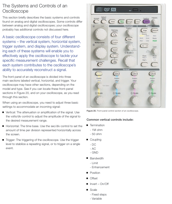
Applicable oscilloscopes: specifically designed for Tektronix TDS3000 series (such as TDS3054, TDS3012) and TDS500 series digital oscilloscopes;
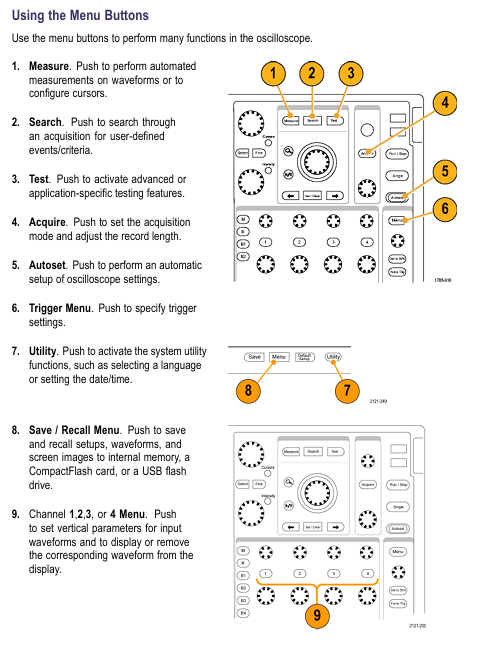
Core positioning: Compact high impedance passive probe, suitable for voltage signal measurement, especially suitable for probe accessories with a size of 3.5mm;
Safety operation standards (ensuring the safety of personnel and equipment)
1. Core security principles
Prohibited live operation: Do not plug or unplug the probe/test line when connected to a voltage source to avoid electric shock or equipment damage;
Terminal rating: The voltage/current rating of each terminal of the probe must be followed (such as the maximum input voltage CAT II 300V RMS), and cannot exceed; The common terminal is at ground potential and is prohibited from connecting high voltage;
Personnel qualifications: Only qualified technicians can perform maintenance procedures, and ordinary users are prohibited from disassembling probes;
Environmental restrictions: Do not use in damp, condensing, or explosive environments; Do not operate in environments with conductive pollutants (pollution level 2).
2. Safety terms and symbols
Application scenarios of terminology/symbol meanings
Warning signs may cause personal injury or death. “Touching the metal part of the probe may result in electric shock
CAUTION labeling may result in equipment/property damage, as “cleaning with benzene solvents may damage the casing”
DANGER identification of immediately accessible injury risks (such as high voltage) probe high voltage terminal labeling
Grounding symbol protection grounding terminal probe grounding terminal identification
Refer to Manual for detailed information on probe body labeling
3. Cleaning and maintaining safety
Cleaning method: Only use a soft cloth dipped in “mild cleaner+water” or “isopropanol” to wipe the probe housing and remove dirt;
Prohibited solvents: Benzene, toluene, xylene, acetone and other solvents should not be used to avoid corrosion of the shell;
Component protection: Avoid liquid infiltration into the probe during cleaning to prevent circuit short circuits.
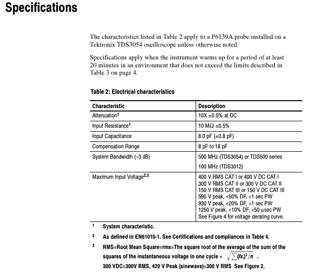
Product features and operating points
1. Core product features
Characteristic Description Application Value
Attenuation ratio of 10X (± 0.5% DC) expands the measurement range of the oscilloscope and adapts to high voltage signals
The cable length of 1.3 meters provides sufficient measurement distance to reduce interference with the tested circuit
Input impedance 10M Ω (± 0.5%)+8.0pF (± 0.8pF) High impedance reduces signal load effect, low capacitance adapts to high-frequency signals
Accessory compatibility compatible with Tektronix 3.5mm probe accessories that can be paired with hooks, grounding leads, etc., to meet various measurement scenarios
2. Key operation: Probe compensation
Due to differences in input capacitance among different oscilloscopes, probe compensation must be performed when replacing the oscilloscope to avoid distortion of low-frequency signals. The compensation steps are as follows:
Connect the probe to the calibration signal output terminal on the front panel of the oscilloscope (usually a 1kHz square wave);
Press the “AutoSet” button on the oscilloscope, or manually adjust to make the screen display clear square waves (1ms/division mode);
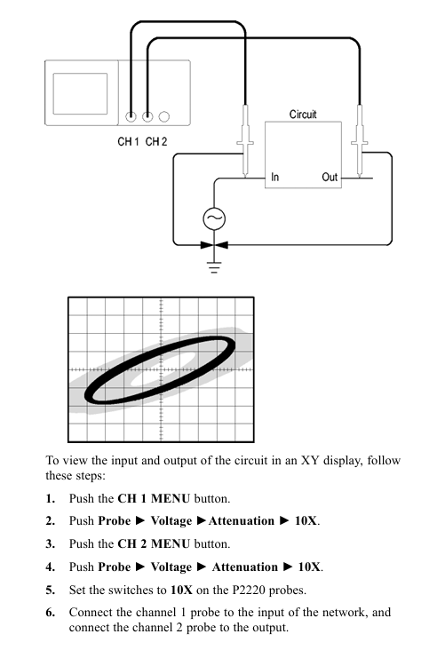
Rotate the micro adjuster using the included adjustment tool (003-1433-02) through the probe “compensation box opening” until the screen displays a completely flat square wave (without overcompensation/undercompensation, as shown in Figure 1).
! [Probe compensation waveform] (schematic diagram of “Undercompensated/Overcompensated/Relatively compensated” in the document)
Undercompensated: The square wave front rises and then falls;
Overcompensated: the square wave front falls and then rises;
Proper compensated: The front edge of the square wave is vertical and the top is flat.
The attenuation ratio is 10X ± 0.5% (under DC conditions) and the system characteristics require the use of an adaptive oscilloscope
Input resistance 10 M Ω± 0.5% high impedance design to reduce signal attenuation
Input capacitance of 8.0 pF ± 0.8 pF, low capacitance suitable for high-frequency signals, reducing phase distortion
Compensation range of 8 pF~18 pF covers the input capacitance range of most oscilloscopes
System bandwidth (-3dB) TDS3054:500 MHz; TDS3012:100 MHz strongly correlated with oscilloscope model
Maximum input voltage CAT I: 400V RMS/DC; CAT II:300V RMS/DC; CAT III: The peak voltage of 150V RMS/DC needs to refer to the duty cycle (e.g. 590V peak when<50% DF)
2. Physical and environmental characteristics
Description of Characteristics and Specifications
Net weight (including accessories)<110 g (0.24 lb) Lightweight design for easy handheld measurement
Temperature range: -15 ℃~+65 ℃ (+5 ℉~+149 ℉); Non work: -62 ℃~+85 ℃ (-80 ℉~+185 ℉) Suitable for laboratory and industrial environments
Humidity 5 cycles (120 hours), 95%~97% relative humidity meets Tektronix standard 062-2847-00 Class 3
Altitude<2000 meters to avoid the impact of high altitude and low pressure on insulation performance
When the input impedance curve frequency is 1Hz~10 ⁸ Hz, the impedance and phase characteristics are stable. Figure 3 provides a typical impedance curve
3. Certification and Compliance
The probe complies with multiple international safety standards to ensure compliance for use in different regions
European standards: EN 61010-1/A2 (Safety of measuring equipment), EN 61010-2-031:1994 (Handheld probe components);
North American Standard: UL 3111-1 (First Edition) CSA C22.2 No. 1010.1-92、CSA C22.2 No. 1010.2.031-94;
Pollution level: Pollution Degree 2 (prohibited from use in environments with conductive pollutants);
Overvoltage category: Supports CAT I/CAT II/CAT III (classified according to voltage levels, such as CAT III applicable to distribution systems).
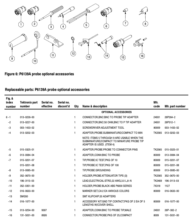
Accessories and Replacement Parts
1. Standard accessories (included with probe)
Accessory Name Tektronix Part Number Function Description
When using multiple probes with color marker tape 016-0633-00, the correspondence between the marker probe and the oscilloscope channel
SMT KlipChip and grounding lead 196-3305-00 connect the probe to a small/hard to reach grounding point
Low inductance grounding component 343-1003-01 (grounding ring)+195-4240-00 (short wire) reduces the inductance of the grounding lead and reduces high-frequency signal distortion
Insulated crocodile clip grounding lead 196-3113-02 probe grounding connection to grounding reference point
Probe protective shell 204-1049-00 protects the probe tip from mechanical damage
2. Optional accessories (extra optional)
Accessory Name, Part Number, Applicable Scenarios
BNC to probe tip adapter 013-0226-00 converts BNC interface signals into probe measurable tip signals
50 Ω BNC to probe adapter 013-0227-00 compatible with BNC signal source with 50 Ω impedance
Micro to small probe adapter 013-0202-03 enables compact probes to be compatible with small probe accessories
IC Test Probes (10 Pack) 015-0201-07 Accurate Measurement of IC Pins
Probe holder 352-0351-00 fixes the position of the probe and is suitable for long-term measurement
SMT KlipChip set (20 pieces) SMG50 batch SMT (surface mount technology) component grounding connection
3. Main replacement parts (for repair and replacement)
Component Name Part Number Remarks
Probe body (including cable) P6139A probe core component, replace as a whole in case of malfunction
Probe tip component (10X) 206-0441-00 contains 8.0pF capacitor and 9M Ω resistor. Replace when the tip is damaged
Grounding ring 343-1003-01 is the core component of the low inductance grounding component
Replace the BNC plug (male) 131-3219-00 when the BNC interface connecting the probe to the oscilloscope is damaged
Spectrum analyzer 1 channel 1 channel standard 9kHz-1GHz, 3-SA3 option extended to 3GHz
2. Key subsystem specifications
(1) Analog channel input and vertical specifications
Input characteristics: Input coupled AC/DC; The input impedance can be selected as 1M Ω (± 1%, typical capacitance 13pF) or 50 Ω (± 1%);
Maximum input voltage: 300VRMS at 1M Ω DC coupling (installation category II), 5VRMS at 50 Ω (peak value ≤± 20V);
Sensitivity range: 1mV/div-10V/div (1-2-5 sequence) at 1M Ω, 1mV/div-1V/div at 50 Ω;
DC gain accuracy: ± 2.5% for 1mV/div, ± 2.0% for 2mV/div, ± 1.5% for 5mV/div and above (an additional 0.1% for every ℃ above 30 ℃);
Bandwidth characteristics: The 1GHz model has a bandwidth of DC-1GHz at 10mV/div-1V/div and DC-150MHz at 1mV/div (different bandwidth models correspond to different voltage bandwidth relationships).
(2) Horizontal specifications
Sampling rate range: up to 5GS/s (1GHz model) when 1-2 channels are enabled, and up to 2.5GS/s when 3-4 channels are enabled;
Time/grid range: 1GHz model 400ps/div-1000s/div, other models 1ns/div-1000s/div;
Long term sampling rate and delay accuracy: ± 10ppm (≥ 1ms time interval);
Record length: 1K, 10K, 100K, 1M, 5M, 10M optional.
(3) Trigger specifications
Trigger type: Supports edge, sequence (B trigger), pulse width, timeout, logic, video (NTSC/PAL, etc.), serial bus (I2C/SPI/CAN, etc.) triggering;
Edge triggered sensitivity: When simulating channel 1mV/div-4.98mV/div, DC-50MHz is 0.75div, and the highest bandwidth is 1.3div;
Video trigger: Supports interlaced/non interlaced systems, can trigger specific fields and lines, compatible with formats such as 480p/720p/1080p;
Trigger holding range: 20ns-8s.
(4) Other key specifications
Display: 11.6-inch TFT capacitive touch screen, 1920 × 1080 resolution, 16.77 million colors, brightness of 450cd/m ²;
I/O ports: 1 Ethernet (10/100Mb/s), optional GPIB (TEK-USB-488 adapter), 1 HDMI, 3 USB hosts (2 front and 1 rear), 1 USB device;
Environmental adaptability: working temperature -10 ℃ -+55 ℃, working humidity 5% -90% (≤ 40 ℃)/5% -60% (>40 ℃ -+55 ℃), working altitude ≤ 3000m;
Power consumption: maximum 130W, power supply voltage 100V-240V ± 10%, frequency 50/60Hz (supports 400Hz ± 10% at 115V).
Performance verification process
1. Verify the prerequisites
The instrument runs continuously for 10 minutes, and the ambient temperature and humidity are within the operating range;
Perform signal path compensation (SPC), and re execute when the temperature changes by more than 5 ℃;
Connect the oscilloscope and testing equipment to the same AC circuit to avoid offset voltage affecting the results.
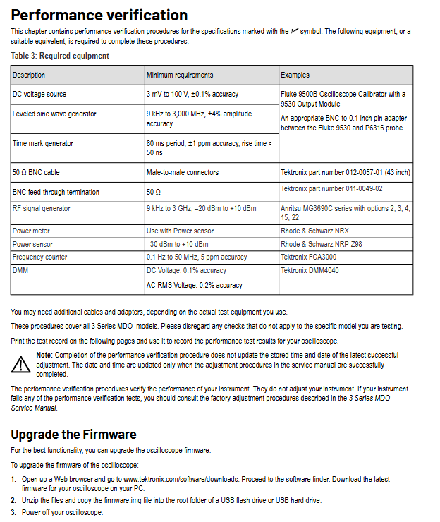
2. Required testing equipment (Table 3)
Minimum requirements for device name, example model
DC voltage source 3mV-100V, ± 0.1% accuracy Fluke 9500B (equipped with 9530 module)
Level sine wave generator 9kHz-3000MHz, ± 4% amplitude accuracy-
Time stamp generator with 80ms cycle, ± 1ppm accuracy, rise time<50ns-
Power meter (including sensor) Power sensor range -30dBm -+10dBm Rohde&Schwarz NRX (with NRP-Z98)
Frequency counter 0.1Hz-50MHz, 5ppm accuracy Tektronix FCA3000
Digital multimeter (DMM) with DC voltage ± 0.1% accuracy and AC RMS ± 0.2% accuracy Tektronix DMM4040
Auxiliary accessories such as 50 Ω BNC cable and 50 Ω BNC straight through terminal Tektronix 012-0057-01 cable
3. Core testing projects and processes
(1) Basic Testing: Self Inspection and SPC
System diagnosis (self-test): Disconnect all probes → press Default Setup → Utility → Self Test → Run Self Test, all items must be “Passed”, failure should contact support;
Signal path compensation (SPC): Default Setup → Utility → Calibration → Run SPC. Each channel takes 5-15 minutes and needs to be “Passed”, otherwise subsequent testing cannot be carried out.
(2) Simulation channel key testing
Key requirements for testing purposes of testing projects
Input terminal testing and verification of 1M Ω/50 Ω input impedance accuracy: 990k Ω -1.01M Ω at 1M Ω, 49.5 Ω -50.5 Ω at 50 Ω (10mV/div, 100mV/div levels)
DC balance test verifies the signal offset of DC coupling at 50 Ω and 20MHz bandwidth. 1mV/div is ± 0.5div, 2mV/div is ± 0.25div, and 10mV/div and above are ± 0.2div
Simulate bandwidth testing to verify the bandwidth compliance at different levels. Under a 50 Ω termination, the gain (Vbw pp/Vin pp) is ≥ 0.707 (-3dB point)
DC gain accuracy test verifies DC signal amplification accuracy of 1mV/div ± 2.5%, 2mV/div ± 2.0%, 5mV/div and above ± 1.5% (20MHz bandwidth, 1M Ω)
Offset accuracy test verifies the accuracy of vertical offset with an error of ± 3.8mV for 1mV/div and 700mV offsets, and ± 0.7V for 1V/div and 100V offsets
(3) Other important tests
Random noise test: In sampling mode, 100mV/div, full bandwidth, 1GHz model ≤ 3.1mV, 100MHz model ≤ 2.85mV;
Time difference measurement accuracy (DTA): When using a 1GHz model with 4ns/div and a 240MHz signal, the error is ≤ 128ps;
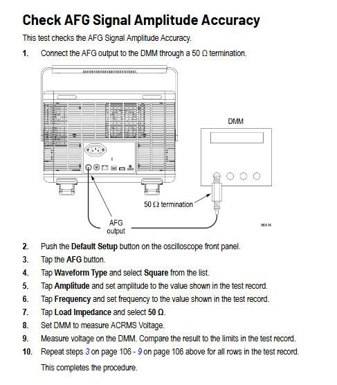
AFG test: sine wave frequency accuracy of ± 1.3kHz at 10kHz, square wave frequency accuracy of ± 1.25kHz at 25kHz, amplitude accuracy of ± 1.5% (1kHz);
DVM test: Error ± 2.052V – ± 1.948V when DC voltage is 1V input, and error ± 0.2mV when AC voltage is 20mVpp (1kHz).
Test records and subsequent processing
Test record: The document provides a detailed table to record the “lower limit value test result upper limit value” for each test, which needs to be printed and filled in;
Result processing: Performance verification only judges whether it meets the standard, without adjusting the instrument; If the test fails, refer to the “3 Series MDO Service Manual” to perform factory calibration;
Calibration cycle: The validity period of the reference frequency error (± 10ppm) is 1 year, and it is recommended to calibrate once a year.
Output impedance: default 50 Ω, can be set to 1 Ω~10k Ω (resolution 1 Ω) or Infinity (>10k Ω).
Modulation types: Supports AM (amplitude modulation), FM (frequency modulation), PM (phase modulation), FSK (frequency shift keying), PWM (pulse width modulation).
Environmental adaptability: working temperature of 0 ℃~40 ℃, humidity of 5%~85% RH, working altitude of 3000m.
Safety regulations and operating taboos
1. Core security principles
Only for professional operation: Only personnel with high voltage/high frequency testing qualifications are allowed to operate, and non professionals are prohibited from contacting.
System level security: If connecting to a large system, it is necessary to comply with the security manuals of other components of the system.
Preoperative examination: Before use, verify that the device is functioning properly with a known signal source and prohibit its use for detecting dangerous voltages.
2. Key operations for preventing electric shock and fire prevention
(1) Power supply and grounding
Use designated power cords (must comply with local certification), and do not mix power cords from other devices.
The equipment is grounded through the power cord, and the grounding conductor must be connected to the ground. It is forbidden to disconnect the grounding connection.
Confirm that the power supply voltage matches the rated value of the equipment (such as 100V~240V AC) before powering on.
(2) Connection/disconnection sequence
Operation type, step purpose
Connect circuit 1. Connect the probe output to the measuring instrument → 2 Connect the probe reference terminal to the tested circuit → 3 Connect the probe input to avoid electric shock or equipment damage caused by live plugging and unplugging
Disconnect circuit 1. Disconnect probe input and reference terminal → 2 Disconnect the probe from the instrument to prevent residual voltage shock
(3) Taboos on Environment and Equipment Status
Do not use in damp, explosive, and dusty environments, and do not operate without cover plates/panels (exposing high-voltage circuits).
If the equipment falls, gets wet, or is suspected of damage, authorized personnel must inspect it before use, and it is prohibited to disassemble it by oneself.
Do not touch the exposed circuit when powered on, and keep the probe body and output line away from the tested circuit.
Remote control interface and instruction system
1. Interface configuration
(1) GPIB interface
Requirements:
Each device must have a unique address (1-30) and must not be duplicated;
The bus can connect up to 15 devices, with a total cable length of ≤ 20m and at least 1 device per 2m;
Power on devices account for ≥ 67%, support star/linear topology, and prohibit parallel/ring topology.
Address setting: Enter the address through the panel “Utility → I/O Interface → GPIB Address” (* RST command cannot initialize the address).
(2) VISA interface
TekVISA software (official website download) needs to be installed, supporting GPIB, RS-232, Ethernet remote control, and complying with VISA 2.2 standard.
Applicable development environment: Windows system, supporting ADE (Application Development Environment) such as LabVIEW and VB.
SCPI command SOURce1: FUNCTION SIN, OUTPut1: STATe ON. Set the waveform of channel 1 to sine and enable the output of channel 1
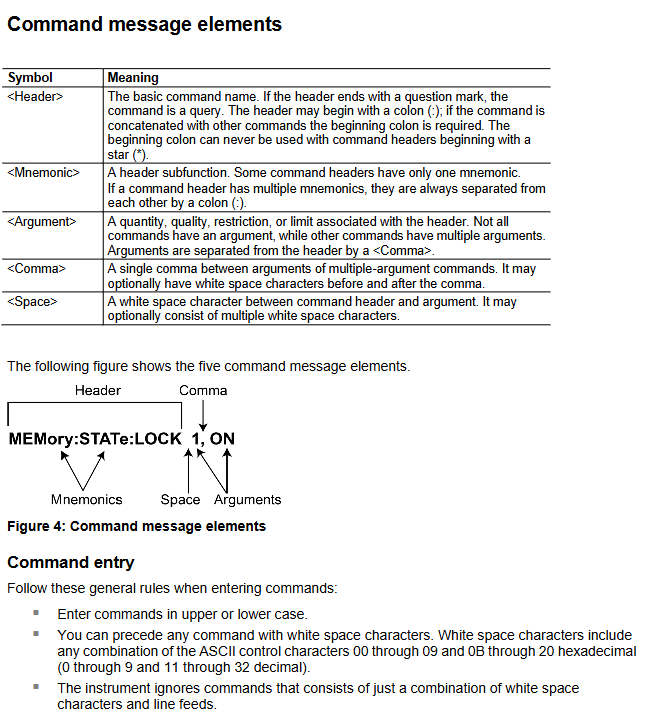
(2) Core Grammar Rules
Abbreviation: Commands can be abbreviated (uppercase is required, lowercase can be omitted), such as DISPlay: BRIGhtness can be abbreviated as DISP: BRIG.
Chain command: Multiple commands are separated by semicolons, and prefixes can be omitted for the same root node, such as TRIGger: CLOPe POS; SOURce SIN (assuming the trigger slope is positive and the source waveform is sine).
SI units: support voltage (V/mV), frequency (Hz/kHz/MHz), time (s/ms/μ s/ns), etc., such as Frequency 10MHz (assuming frequency 10MHz).
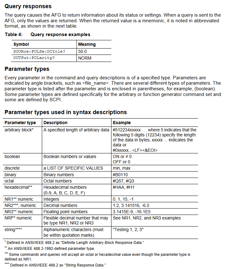
Parameter type: Supports Boolean values (ON/OFF), numerical values (NR1/NR2/NR3), and strings (quotation marks required), such as MMEMory: DELete “U:/TEST. TFWX” (remove the TEST. TFWX file from USB).
Detailed explanation of core functions and instructions
1. Waveform generation and output control
(1) Waveform type and parameter settings
Supporting waveforms: 13 types including sine (SINusoid), square wave (SQUare), pulse (PULSe), ramp (RAMP), noise (PRNoise), arbitrary wave (EMEMory/EFILe), etc.
Example of Key Instructions:
Let the waveform of channel 1 be sine: SOURce1: FUNCTION SIN
Assuming a frequency of 10kHz: SURce1: Frequency 10kHz
Set amplitude to 2Vpp: SURce1: VOLTage: Amplitude 2VPP
Turn on AM SOURce1: AM: STATe SOURce1: AM: STATe ON
3. Sequence control (advanced mode)
Support defining 256 sequence elements to achieve waveform looping, jumping, and waiting for triggering. Core instructions:
New sequence: SEQueen: NEW
Set sequence length (10 elements): SEQuence: LENGth 10
Let element 1 loop 100 times: SEQuence: ELEM1: LOOP: COUNT 100
After triggering element 1, jump to element 6: SEQuence: ELEM1: GOTO: INDex 6; GOTO:STATe ON
Running sequence: SEQControl: RUN: IMMediate
4. Data storage and management
(1) Virtual Disk Definition
Disk identification, storage location, permission usage
U: USB flash storage for reading and writing user waveforms/settings files
M: Internal flash read-write storage commonly used waveforms/settings
P: Internal predefined area read-only storage factory preset waveforms (such as sine and square waves)
(2) Store/load instructions
Save channel 1 waveform to USB: MMEMory: STORe: TRACe EMEMory1, “U:/WAVE1. TFWX”
Loading settings from USB to memory 1: MMEMory: LOAD: STATe 1, “U:/SET1. TFS”
Delete USB file: MMEMory: DELete “U:/OLD. TFWX”
Status and Event Management
1. Status register system
Compliant with IEEE 488.2 and SCPI standards, the core registers are as follows:
Meaning of register name function key bits
Status Byte Register (SBR) summarizes device status OSB (operational status), ESB (event status), MAV (message available)
The Standard Event Status Register (SESR) records core events OPC (operation completed), CME (command error), EXE (execution error)
The operating condition register (OCR) records the operating status CAL (calibration in progress), SWE (scanning in progress), WTRIG (waiting for trigger)
2. Error code system
Error codes are divided into “standard errors” (-100~-499) and “device specific errors” (1~32767). Common examples include:
Error code type description
-100 command errors command syntax errors (such as spelling errors)
-222 execution error parameter out of range (e.g. frequency set to 1000MHz, exceeding the upper limit of 250MHz)
-350 device error error queue overflow (more than 64 events)
2305 self-test error CH1 output gain self-test failed
3. Error query
Search for the next error: SYSTem: ERRor: NEXT? The return format is -222, “Data out of range”
Maintenance and troubleshooting
1. Maintain standards
Cleaning: Wipe the outer surface with a dry lint free cloth or 75% isopropanol. Do not use water/solvents/abrasives, and do not allow moisture to enter the interior of the equipment.
Repair restriction: There are no user repairable parts, and only DC offset can be adjusted for serial numbers C019999 and below. Other faults need to be returned to the factory.
2. Common fault handling
Troubleshooting steps for possible causes of fault phenomena
No waveform output turned on, parameter out of range 1. Execute OUTPut1: STATe? Confirm the output status; 2. Check if the frequency/amplitude is within the device range
GPIB no response address conflict, cable fault 1. Confirm that GPIB address is unique; 2. Replace GPIB cable; 3. Restart the device and controller
Calibration failed due to excessive temperature and humidity in the environment, hardware malfunction. 1. Confirm that the environment is 0 ℃~40 ℃/5%~85% RH. 2. Execute DIAGnostic? Self inspection; 3. If errors 1101-1216 are reported, return to the factory for repair
Compliance Information and Environmental Requirements
1. EMC (Electromagnetic Compatibility) compliance
Core Directive: Complies with the requirements of EU Directive 2004/108/EC.
Key criteria:
Emission standards: EN 61326-1:2006, EN 61326-2-1:2006, CISPR 11:2003 (Group A, Radiation and Conducted Emissions);
Immunity standard: IEC 61000-4 series (electrostatic discharge, radio frequency electromagnetic field, electrical fast transient, power surge, voltage sag, etc.);
Power standards: EN 61000-3-2:2006 (harmonic emission), EN 61000-3-3:1995 (voltage fluctuation and flicker).
Special note:
Only for non residential use, residential use may generate electromagnetic interference;
When connecting the tested object, it may exceed the standard emission limit, and high-quality shielded interface cables should be used to ensure compliance.
2. Safety compliance standards
Compliance Area Core Standards Applicable Requirements
EU Low Voltage Directive 2006/95/EC, EN 61010-031/A1:2008 Safety Requirements for Handheld Measurement Probes
Canadian CAN/CSA-C22.2 No.61010-031-07/A1:2010 has equivalent requirements to EN 61010-031/A1:2008
International General IEC 61010-031/A1:2008 Safety Specification for Electrical Equipment for Measurement, Control and Laboratory Use
3. Environmental requirements
Pollution level: rated as level 2 (normal environment only contains dry non-conductive pollution, occasional temporary conductivity may occur due to condensation, typical office/home environment, condensation may occur when the product is stopped), limited to indoor use only.
Measurement category definition:
CAT I: Measurement of circuits not directly connected to the power grid;
CAT II: Circuit measurement directly connected to low-voltage power grid;
CAT III: Measurement of power distribution systems inside buildings;
CAT IV: Low voltage power grid source measurement (three probes support up to CAT III, the specific level depends on the model and accessories).
Environmental compliance:
Compliant with EU WEEE (2002/96/EC) and Battery Directive (2006/66/EC), requiring recycling and disposal through compliant channels;
Classified as monitoring and control equipment, exempt from RoHS (2002/95/EC) directive requirements.
Product model parameters and core characteristics
1. Comparison Table of Core Parameters of Three Probes
Input resistance difference: 40M Ω± 2%; Single end to ground: 10M Ω± 2%/side differential: 10M Ω± 2%; Single end to ground: 2.5M Ω± 2%/side differential: 5M Ω± 2%; Single end to ground: 1.25M Ω± 2%/side
Input capacitance difference:<2.5pF; Single end to ground:<5.0pF/side difference:<2.0pF; Single end to ground:<4.0pF/side difference:<2.0pF; Single end to ground:<4.0pF/side difference
Common mode rejection ratio (CMRR) DC:>80dB; 100kHz:>60dB; 3.2MHz:>30dB; 100MHz:>26dB Same as THDP0100 Same as THDP0100
Maximum common mode voltage/ground voltage ± 6000V (DC+peak AC); 2300V CAT I; 1000V CAT III ± 1500V (DC+peak AC); 1000V CAT II; 600V CAT III ± 750V (DC+peak AC); 550V CAT I; 300V CAT III
Input overload recovery time in 600V range:<30ns (recover to the final value of 10% after 5 times overload); 6000V gear:<30ns 150V gear:<20ns 1500V gear:<20ns 75V gear:<20ns 750V gear:<20ns
Operation Guide: Connection, Control, and Measurement
1. Connect to the measuring instrument (oscilloscope)
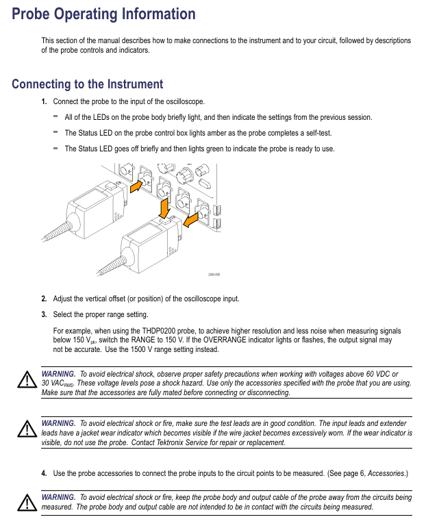
Physical connection: Insert the probe into the input channel of the oscilloscope, and all LEDs of the probe will briefly turn on and then return to the previous usage settings; The Status LED on the control box first turns amber (during self check), briefly goes off, and then turns green, indicating that the probe is ready.
Oscilloscope settings: Adjust the vertical offset (position) of the oscilloscope input, and select the appropriate probe range based on the measured signal voltage (low range has higher resolution and less noise, and high range needs to be switched when exceeding the range).
Security check: Confirm that the input impedance of the oscilloscope is 1M Ω and the bandwidth is not lower than the probe bandwidth; When the voltage is greater than 60VDC or 30VAC RMS, it is necessary to check again whether the accessory connections are secure.
2. Connect to the tested circuit
Connection line selection: Use the probe’s built-in integral input line (25.4cm) or extension line (1.5m, paired to ensure consistent line length and reduce noise and inductance effects).
Accessory connection: Select accessories (such as hook tips, clamps, etc.) based on the type of test point, first connect the accessories to the probe input line, ensure a secure connection, and then connect them to the test circuit; Do not directly connect the voltage source when the accessory is not connected to the probe.
Measurement distance: Extending the cable can increase the distance between measurement points to 3.5m, but the measurement accuracy will decrease when the frequency is greater than 10MHz. It is recommended to use an oscilloscope with a bandwidth filter of 20MHz or below.
3. Detailed explanation of probe controls and indicator lights
Function description of control/indicator light position
Press the probe release button on the control box to unlock the connection between the probe and oscilloscope. First, disconnect the circuit and then unplug the probe
Status LED control box amber: self-test in progress; Green: Normal ready; Amber/Red: self-test failure or malfunction
The MENU button control box brings up the probe setting menu on the oscilloscope, which can operate functions such as AutoZero and range selection
The voltage range (RANGE) button and LED probe head switch between low/high range, and the LED displays the current range; Overrange LED lights up when exceeding the limit
BANDWIDTH LIMITED button and LED probe head switch to full bandwidth/5MHz limit; 5MHz can filter out high-frequency noise and harmonics in switch mode power supplies, suitable for SMPS testing
Overrange indicator light: The probe head of the probe lights up red: the differential signal exceeds the linear range of the current range, and the output signal is inaccurate
AUDBLE OVERRANGE button and LED probe head switch over range buzzer function (default enabled); ON/OFF LED indicates the current status
4. Key precautions for measurement
Limitations of Over Range Detection: OVERRANGE only detects differential over range between+/- inputs and does not detect common mode voltage or ground voltage over range. It is necessary to confirm that there is no over range situation through single ended measurement (ground at the – end and ground voltage at each point at the+end).
Common mode signal suppression: Twisted pair input lines can reduce noise coupling in high EMI environments; The higher the frequency, the lower the common mode rejection ratio, and the accuracy of the signal needs to be evaluated based on the measured frequency.
Probe load effect: The probe will introduce resistance, capacitance, and inductance into the tested circuit. When the frequency is greater than 1kHz, the input impedance decreases, and the load effect of low impedance and low-frequency signals can be ignored.
Accessory System: Standard Configuration and Optional Accessories
1. Standard accessories (by model)
(1) THDP0100 standard accessories
Accessory Name, Specification, Parameter Quantity, Revised Model
Extension cable length 1.5m, banana plug, 1000V CAT III, 600V CAT IV 1 pair 196-3523-xx
Test probe (TATP) 6-32 threaded head, with finger protection, 2300V CAT I, 1000V CAT II 1 pair included in 020-3070-xx kit
TASH compatible TATP for small conductors, 2300V CAT I, 1000V CAT II 1 pair included in 020-3070-xx kit
TALH compatible TATP for bolt terminals and busbars, 2300V CAT I, 1000V CAT II 1 pair included in 020-3070-xx kit
(2) THDP0200&TMDP0200 standard accessories
Accessory Name, Specification, Parameter Quantity, Revised Model
Extension cable length 1.5m, banana plug, 2300V CAT I, 1000V CAT III 1 pair 196-3523-xx
Crocodile clip (344-0670-xx) double insulated, suitable for large bolts/busbars, 1000V CAT III, 10A 1 pair 344-0670-xx
The probe holder (TPH1000) supports hands-free measurement with handheld probes and requires one TPH1000 rubber foot
THV Browser adjusts the distance between two probes (maximum 2.54cm), supports one handed browsing or hands-free measurement of one THV Browser
2. Optional accessories
Accessory Name, Function, Usage, Re order Model
TekVPI calibration fixture provides probe power supply and routes output signals to SMA interface for performance verification and gain adjustment 067-1701-xx
Replace the label (safety component) to cover the repair adjustment hole on the back of the probe, and replace it after repair to ensure safety 335-2913-xx
3. Restrictions on the use of accessories
The test probe and hook tip of THDP0100 are prohibited from being used in CAT III/IV circuits; When used in conjunction with THDP0200/TMDP0200, it is prohibited to use it on circuits with voltages greater than 1000V.
The spring needle tip adapter and the extended test probe adapter will lower the probe voltage level, and their rated voltage (150V CAT II/300V CAT II) must be strictly followed.
When using TP175-FL for CAT III circuit measurement, the probe tip should be retracted (approximately 3.7mm of exposed metal) to prevent arc flashover.
Functional inspection and calibration process
1. Function check (quick verification of probe availability)
(1) Preparation for Inspection
Equipment: Oscilloscope, AC power supply, probe standard accessories.
Prerequisite: When the accessories are fully connected and the voltage source is greater than 42Vpk, it is necessary to confirm that the connection is firm.
(2) Inspection steps and judgment criteria
Input 1 (+/-) Input 2 (-/+) Measurement mode range setting check standard
High range (6000V/1500V/750V) oscilloscope display line voltage with no significant distortion for live wire ground/neutral wire differential
The live/neutral differential low range (600V/150V/75V) oscilloscope displays the line voltage, and the OVERRANGE light lights up when the input exceeds the range by about 20%
No signal display on the common mode high/low range oscilloscope with live wire (same connection point) (AutoZero is required to offset DC offset)
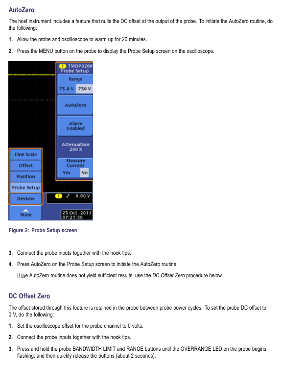
2. Calibration operation (including AutoZero and offset adjustment)
(1) AutoZero (offsetting DC offset)
Preheating: Connect the probe and oscilloscope to power for 20 minutes.
Short circuit input: Use the hook tip to short-circuit the probe+/- input.
Start calibration: Press the probe MENU button, select “AutoZero” from the “Probe Setup” menu on the oscilloscope, and wait for calibration to complete.
(2) DC offset zero adjustment (manual)
Oscilloscope setting: Set the vertical offset of the probe channel to 0V.
Short circuit input: Use a hook tip to short-circuit the probe+/- input.
Enter adjustment mode: Long press the BANDWIDTH LIMITED and RANGE buttons on the probe for about 2 seconds until the OVERRANGE LED flashes and then release.
Adjust the zero position: Use the BANDWIDTH LIMITED and RANGE buttons to adjust the offset voltage displayed on the oscilloscope to 0V.
Storage settings: Press the AUDBLE OVERRANGE button, the OVERRANGE LED stops flashing, and the settings take effect.
Repeat: Switch to another range and repeat steps 3-5.
(3) DC offset zero reset (restore default)
Short circuit input: Use a hook tip to short-circuit the probe+/- input.
Enter reset mode: Long press the BANDWIDTH LIMIT and RANGE buttons for about 4 seconds until the OVERRANGE LED stays on, then release.
Store default value: Press the AUDBLE OVERRANGE button, the OVERRANGE LED will turn off, and the default offset value will be restored.
Repeat: Switch to another range, repeat steps 2-3, and then perform DC offset zero adjustment again.
Oscilloscope channel connected to calibration fixture → probe output connected to calibration fixture, probe input connected to signal generator through adapter;
The SMA interface of the calibration fixture is connected to the DMM through a coaxial cable, and the DMM is set to AC voltage mode.
Parameter setting and measurement (adjusted by model)
|Probe model | Range | Generator setting (100Hz square wave) | Expected DMM reading (rms) | Qualified range|
Turn off generator output → Set probe range and generator parameters → Turn on generator → Record DMM reading → Turn off generator → Switch range and repeat measurement.
Connect the probe to the oscilloscope and keep the input line straight and parallel.
Parameter settings:
Pulse generator: 50V output, 1kHz frequency, 200ns pulse width (probe input actual 25V, due to 2X attenuation);
Oscilloscope: 5V/div, 10ns/div, full bandwidth, average of 16 samples;
Probe: Full bandwidth, corresponding range.
Measurement and Qualification Standards:
Turn on the generator and use an oscilloscope to automatically measure the rise time → record the value → switch the range and repeat the measurement;
Qualification criteria: THDP0100 range ≤ 3.6ns; THDP0200 150V range ≤ 2.4ns, 1500V range ≤ 2.0ns; TMDP0200 75V range ≤ 2.4ns, 750V range ≤ 2.0ns.
4. Internal adjustment (limited to probes with serial number C020000 and above)
(1) Adjustment premise
The safety label on the back of the probe needs to be removed (must be replaced after repair) and an insulation adjustment tool should be used.
Preheat for 20 minutes before adjustment, strictly follow the high-voltage operation specifications (professional personnel are required for voltage>30VAC RMS).
(2) Adjustable projects and processes
Adjust the reference standards for the core steps of the project
Gain accuracy 1. Connect the calibration fixture, generator, and DMM; 2. Verify parameter settings based on gain accuracy; 3. Use insulation tools to adjust the DC gain potentiometer of the corresponding range, so that the DMM reading is within the qualified range and meets the gain accuracy verification standard (± 2%)
DC CMRR 1. Connect the two inputs of the probe to the generator+terminal, and set the generator parameters according to the table; 2. Set the oscilloscope to 10ms/div and 5MHz bandwidth; 3. Adjust the DC CMRR potentiometer to minimize the signal amplitude displayed on the oscilloscope. The signal amplitude should be minimized without significant fluctuations
LF compensation 1. Probe input connected to generator for fast rising edge output (10kHz, 50Vp-p); 2. Set the oscilloscope to 4 μ s/div, averaging 16 times; 3. Adjust in the order of “long+LF → long+LF * → short+LF” (TMDP0200 without+LF *); 4. Reverse the input line and adjust the square wave response optimization by pressing “Long LF → Long LF * → Short LF”, without overshoot or attenuation
AC CMRR 1. Connect the two inputs of the probe to the generator+terminal, and set the generator to 297Vp-p (105Vrms) and 100kHz; 2. Set the oscilloscope to 10 μ s/div and probe to full bandwidth; 3. Fine tune+LF potentiometer (short+LF → long+LF → long+LF *) to minimize signal amplitude. The signal amplitude is minimized, and CMRR conforms to typical values
(3) DC CMRR generator parameter settings
Probe Model Range Generator Voltage (rms) Generator Voltage (p-p) Frequency
THDP0100 600V 353.53V 1000V 40Hz
THDP0200 150V 200V 566V 40Hz
TMDP0200 75V 353.53V 1000V 40Hz
Troubleshooting and Maintenance
1. Common faults and solutions
Troubleshooting steps for possible causes of fault phenomena
The probe LED does not light up frequently. There are interface and channel faults between the probe and oscilloscope. 1. Disconnect and reconnect the probe; 2. Replace the oscilloscope channel; 3. Restart the oscilloscope and reconnect it; 4. Replace the oscilloscope for testing (if the fault follows the probe, it needs to be returned to the factory)
The oscilloscope has no signal and the display accessories are not fully connected, the probe and circuit are loose, and the probe is faulty. 1. Check whether the accessory connections are firm (banana plugs and clamps need to be fully inserted); 2. Reconnect the probe to the tested circuit and confirm good contact; 3. Perform functional checks to verify if the probe is functioning properly; 4. Check the oscilloscope channel settings (such as coupling mode and range)
The OVERRANGE light is abnormally on, and the differential signal is out of range and the common mode voltage/ground voltage is out of range. 1. Switch to a higher range and observe if the light goes out; If it is already at the highest range, stop measuring and check the measured signal; 3. Perform single ended measurement to confirm that the common mode voltage and ground voltage do not exceed the rated value of the probe
Measurement signal distortion: Insufficient probe bandwidth, input line not twisted, load impact: 1. Confirm that probe bandwidth is ≥ measured signal frequency; 2. Twist the input line to reduce noise coupling; 3. Evaluate the impact of probe load on the tested circuit and replace the high input impedance probe if necessary
The gain accuracy probe is not calibrated and the environmental temperature and humidity exceed the standard. 1. Perform AutoZero calibration; 2. Re calibrate the gain according to the performance verification process; 3. Confirm that the measurement environment is within the range of 0 ℃~40 ℃ and 5%~85% RH
2. Firmware upgrade
If the oscilloscope does not display all probe controls/indicator lights or frequently malfunctions, it may be necessary to upgrade the oscilloscope firmware.
3. Maintenance and upkeep standards
(1) Cleaning requirements
Cleaning tools: dry lint free cloth, soft bristled brush; Wipe stubborn stains with a cloth/cotton swab dampened with 75% isopropanol.
Prohibitions: It is prohibited to use spray, liquid solvent and abrasive; Prohibit moisture from entering the interior of the probe; Do not clean the internal components of the probe.
(2) Maintenance restrictions
There are no user repairable parts. Probes with serial number C019999 and below can only perform AutoZero and DC offset adjustment. Other faults need to be returned to the factory.
Repair request: Contact a Tektronix service representative or authorized repair center to return the product for repair according to the instructions.
Key usage risks and avoidance suggestions
High voltage electric shock risk: Strictly follow the connection/disconnection sequence, use designated accessories, wear insulation protective equipment when the voltage is greater than 60VDC/30VAC RMS, and do not touch exposed circuits.
Risk of probe damage: Do not use beyond the range or environmental conditions; Unauthorized disassembly and assembly are prohibited; Prohibit the use of worn or non certified accessories.
Measurement error risk: Perform AutoZero calibration before measurement; Pay attention to the decrease of common mode rejection ratio during high-frequency measurement; When using an extension cable, it should be paired with a low bandwidth filter; Regularly (1 year) conduct performance validation.
Environmental safety risks: Do not use in damp, explosive, and dusty environments; Ensure good heat dissipation of the probe and avoid prolonged high-temperature operation.
The specification and performance verification manual for the Tektronix 3 series hybrid domain oscilloscope (with 2 channels for MDO32 and 4 channels for MDO34) covers three major modules: hardware parameters (analog bandwidth of 100MHz-1GHz, maximum sampling rate of 5GS/s, and 16 optional digital channels), multi domain functionality (oscilloscope+spectrum analyzer+arbitrary function generator+digital voltmeter), and performance verification process (20+tests including input impedance, DC balance, analog bandwidth, etc.). The key indicator range is clearly defined (such as maximum input voltage of 300VRMS, display average noise level ≤ -109dBm/Hz), and standardized testing steps are provided (including required equipment list, wiring diagram, data recording table), while emphasizing safety specifications (CAT II). Provide complete technical guidance for instrument calibration, troubleshooting, and compliance verification, including installation category and grounding requirements.
Model differences and core parameters
Model Features MDO32 (2 channels) MDO34 (4 channels) Remarks
Analog bandwidth 100MHz-1GHz 100MHz-1GHz model sampling rate 5GS/s, other 2.5GS/s
Digital channel 16 channels (3-MSO option) 16 channels (3-MSO option) input capacitor 8pF, minimum signal swing 500mVpp
4. Parameters of any function generator (3-AFG option)
Parameter specifications
13 types of output waveforms including sine wave, square wave, pulse, and ramp
Frequency range: sine wave 0.1Hz-50MHz; Square wave 0.1Hz-25MHz
Range of amplitude 50 Ω load: 10mVpp-2.5Vpp; High resistance load: 20mVpp-5Vpp
DC offset ± 1.25V (50 Ω); ± 2.5V (high resistance)
Rise/fall time 5ns (10% -90%, square wave)
Distortion sine wave ≤ 1% (50 Ω, 1kHz)
Performance verification process
1. Verify the prerequisites
The instrument needs to be preheated in an environment of 18 ℃ -28 ℃ for at least 10 minutes;
Perform signal path compensation (SPC) (path: Utility → Calibration → Run SPC), if the temperature change exceeds 5 ℃, it needs to be re executed;
The oscilloscope and testing equipment need to be connected to the same AC power circuit (to avoid errors caused by ground offset).
2. Core test items and steps (example)
Qualification criteria for key steps of testing equipment in testing projects
Input impedance (1M Ω/50 Ω) DC voltage source, impedance measuring instrument 1. Connect the voltage source to channel 1; 2. Set the vertical gear to 10mV/div/100mV/div; 3. Measure impedance values of 1M Ω: 990k Ω -1.01M Ω; 50 Ω: 49.5 Ω -50.5 Ω
DC balanced 50 Ω terminal load 1. Channel connected to 50 Ω terminal; 2. Set the vertical gear to 1mV/div-1V/div; 3. Convert the measurement mean to divisions 1mV/div (50 Ω): ± 0.5div; 2mV/div and above: ± 0.2div
Analog bandwidth sine wave generator 1. Input 10MHz signal (8div amplitude); 2. Adjust to the maximum bandwidth frequency; 3. Calculate the gain (Vbw pp/Vin pp) with a gain ≥ 0.707 (-3dB point)
Random noise free (internal noise) 1. Disconnect all inputs; 2. Set up a 50 Ω terminal with full bandwidth; 3. Measure AC RMS noise at 100mV/div level: 1GHz model ≤ 3.1mV; 100MHz model ≤ 2.85mV
Digital threshold accuracy DC voltage source, P6316 probe 1. Connect the probe to the voltage source; 2. Set a threshold of 0V/4V; 3. Record Vs – (high → low) and Vs+(low → high) 0V: ± 0.1V; 4V: 3.78V-4.22V
3. List of Testing Equipment (Table 3)
Minimum requirements for device name, example model
DC voltage source 3mV-100V, ± 0.1% accuracy Fluke 9500B (equipped with 9530 module)
Sine wave generator 9kHz-3GHz, ± 4% amplitude accuracy Anritsu MG3690C
Power meter+sensor -30dBm -+10dBm Rhode&Schwarz NRX (with NRP-Z98)
Frequency counter 0.1Hz-50MHz, 5ppm accuracy Tektronix FCA3000
Digital Multimeter (DMM) DC ± 0.1%, AC RMS ± 0.2% Tektronix DMM4040
Safety and Maintenance
1. Safety regulations
Grounding requirements: A 3-pin power cord must be used, and the grounding conductor must be reliably connected to the ground. Disconnecting the grounding is prohibited;
Input restrictions: Maximum 300VRMS (CAT II) for 1M Ω channel, maximum 5VRMS for 50 Ω channel, overvoltage may damage terminal resistance;
Operation taboos: Do not plug or unplug probes/cables with power on, do not use in damp (>90% RH) or explosive environments, and do not operate after removing the instrument cover.
2. Maintenance and Calibration
Firmware upgrade: 1 Download firmware. img from the official website to USB; 2. Turn off the oscilloscope and plug it into a USB port; 3. Automatic upgrade upon startup (power off prohibited);
Calibration cycle: recommended to be 1 year, with a reference frequency error accumulation of ± 10ppm/year (including aging and temperature effects);
Self check and diagnosis: Path: Utility → Self Test. If it fails, it will enter extended diagnosis and can be exited by pressing MENU OFF (it can be temporarily used when the fault does not affect the measurement).
Key issue
Question 1:3: The simulated bandwidth of the 3 series MDO is related to the vertical gear. What is the actual bandwidth of the 1GHz model at different vertical gears? How to confirm whether the bandwidth is qualified through performance verification?
Answer:
1、 Actual bandwidth of different vertical gears for 1GHz models
The simulated bandwidth of the 1GHz model decays with decreasing vertical gear, and the specific corresponding relationship is as follows:
2、 Bandwidth performance verification steps (taking 50 Ω input as an example)
Equipment connection: Connect a sine wave generator (such as Fluke 9500B) to oscilloscope channel 1 via a 50 Ω coaxial cable, with the generator output impedance set to 50 Ω;
Oscilloscope settings:
Reset according to Default Setup;
Set the Acquisition Mode to Sample;
Add peak to peak measurement (Measure → Amplitude → Peak to Peak → Add);
Channel 1 setting: Termination=50 Ω, Vertical Scale=corresponding test gear (such as 1mV/div);
Signal input: The generator outputs a 10MHz sine wave, adjust the amplitude to display 8div on the screen (such as outputting 8mVpp at 1mV/div level), and record the peak value (Vin pp) at this time;
Bandwidth test: Adjust the generator frequency to the maximum bandwidth corresponding to this gear (e.g. 1mV/div corresponds to 150MHz), and record the peak value (Vbw pp) at this time;
Qualification judgment: Calculate the gain as Vbw-pp/Vin pp. If the gain is ≥ 0.707 (-3dB point), the bandwidth is qualified.
Question 2: How to test the threshold accuracy of the digital channel (3-MSO option) of the 3 series MDO? What are the key operational details to pay attention to during testing?
Answer:
1、 Testing steps for threshold accuracy of digital channels
Equipment preparation: DC voltage source (such as Fluke 9500B), P6316 digital probe, BNC-to-0.1 inch pin adapter;
Probe connection: P6316 probe Group 1 is connected to a voltage source, and an adapter is used to match the interface;
Oscilloscope settings:
Reset according to Default Setup;
Activate the digital channel (D15-D0 button → Turn All On);
Set digital channel threshold (such as 0V or 4V): D15-D0 menu → Thresholds → Enter target value;
Trigger setting: Trigger → Source=Target digital channel (such as D0), Slope=Rising/Falling;
Threshold measurement (taking 0V threshold as an example):
Vs – (high to low switching voltage): Set the voltage source to -400mV, gradually increase by 20mV until the channel displays a stable low level (blue), and record the voltage as Vs – at this time;
Vs+(low to high switching voltage): Set the voltage source to+400mV, gradually -20mV until the channel displays a stable high level (green), and record the voltage as Vs+at this time;
Calculate the average threshold: VSAvg=(Vs -+Vs+)/2;
Qualification judgment: The 0V threshold must meet the requirement of * * -0.1V ≤ VSAvg ≤ 0.1V * *, and the 4V threshold must meet the requirement of 3.78V ≤ VSAvg ≤ 4.22V.
2、 Key operational details
Probe grounding: All 8 grounding channels of P6316 probe need to be connected to user grounding to avoid threshold deviation caused by poor grounding;
Voltage stepping: After adjusting the voltage each time, wait for 3 seconds to ensure that the channel state is stable before recording to avoid transient interference;
Trigger slope switching: When measuring Vs -, use the Rising slope, and when measuring Vs+, use the Falling slope to ensure that the trigger point is consistent with the level switching;
Multi channel testing: After testing each channel (such as D0), set its Display to Off and activate the next channel (such as D1) to avoid interference between channels.
Question 3: How to test the display average noise level (DANL) in the spectrum analyzer function of the 3 series MDO? What are the DANL qualification standards for different frequency ranges?
Answer:
1、 DANL testing steps (no input signal, only 50 Ω terminal required)
Equipment connection: oscilloscope RF input connected to 50 Ω feedthrough terminal, no external signal input;
Oscilloscope settings:
Reset according to Default Setup;
Activate RF channel (RF button → On);
Set Trace mode: RF menu → Traces → Average=On, Normal=Off;
9kHz-50kHz: Orizontal → Start=9kHz, Stop=50kHz, move the Marker (Multipurpose knob a) to the highest noise point, and record the DANL value;
50kHz-5MHz:Start=50kHz,Stop=5MHz,Center=2.525MHz, Record the highest noise level;
5MHz-2GHz (3-SA3 option): Start=5MHz, Stop=2GHz, Center=1GHz, Span=10MHz, record the highest noise value;
2GHz-3GHz (3-SA3 option): Start=2GHz, Stop=3GHz, Center=2.5GHz, Span=10MHz, record the highest noise value;
Data processing: Ignore stray signals above the noise level (refer to the “residual response” specification) and only record the noise baseline value.
2、 DANL qualification standards for different frequency ranges
Frequency range standard (without 3-SA3) 3-SA3 option typical values (better than standard)
9kHz-50kHz ≤-109dBm/Hz ≤-109dBm/Hz ≤-113dBm/Hz
50kHz-5MHz ≤-126dBm/Hz ≤-126dBm/Hz ≤-130dBm/Hz
5MHz-1GHz ≤-136dBm/Hz ≤-136dBm/Hz ≤-140dBm/Hz
1GHz-2GHz – ≤-136dBm/Hz ≤-140dBm/Hz
2GHz-3GHz – ≤-126dBm/Hz ≤-130dBm/Hz
3、 Testing precautions
Terminal matching: A 50 Ω terminal must be used, otherwise impedance mismatch may cause high noise measurement;
Stray elimination: If there is significantly higher than the base noise at a certain frequency point (such as 1.25GHz, 2.5GHz), the noise values on both sides of the noise should be recorded, rather than the noise itself;
Average time: In the low-frequency range (such as 9kHz-50kHz), wait for 60 seconds to ensure that the average trace is stable before reading.
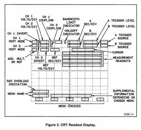
This document is a quick reference guide for the Tektronix 2440 digital oscilloscope, first printed in 1987. Its core positioning is a “practical operation manual” – it does not replace the complete “2440 Operation Manual” (070-6695-00), but focuses on step-by-step operation and menu logic analysis of the instrument’s core functions. The document structure is centered around the “front control panel buttons” and follows the process of “basic power on → functional modules → data output”. It covers 19 key functional chapters, including 19 hardware schematics and menu screenshots, clarifying the hierarchical menu relationship, parameter adjustment range, and typical application scenarios of each button. It is suitable for engineers who have already understood the basic principles of oscilloscopes and need to quickly get started, especially focusing on practical guidance for characteristic functions such as dual trigger systems, multi-mode acquisition, GPIB communication, etc.
Core parameters and hardware layout of the instrument
2.1 Core Technical Parameters
Detailed Explanation of Key System Parameters
Vertical system channel configuration with 2 analog channels (CH1/CH2), supporting ADD/MULT/XY combination mode
Sensitivity range 2mV/div -5V/div (equivalent to 20mV/div -50V/div after 10X probe adaptation)
Coupling method AC/DC/GND, AC coupling and 50 Ω terminal mutually exclusive
The bandwidth limit is adjustable in three levels: 20MHz/100MHz/FULL, and can be extended to 300MHz in Repet mode (only repeating waveforms)
Horizontal system time base range A/B dual time base, 5ns/div -100ms/div, ≤ 100ms/div automatically switches to ROLL mode
Trigger positions 1/8, 1/4, 1/2, 3/4, 7/8, a total of 5 preset positions, supporting GPIB custom positions
Trigger system trigger type A/B dual trigger, supporting Edge/Video/Word/Pulse trigger (Video/Word requires optional)
Coupling method DC/AC/Noise Reject/LF Reject/HF Reject, adapted to different signal noise environments
There are a total of 5 collection modes for the collection system: Normal/Average/Explore/Repet/Save On Delta
Average frequency 2/4/8/16/32/64/128/256 times optional
The storage system has four independent reference memories (REF1-REF4), which support waveform freezing and calling
The GPIB communication interface supports Talk/Lite mode and is compatible with printer/plotter data output
2.2 Core Layout of Front Control Panel (Divided by Function)
(1) Display control area
INTENSITY knob: continuously adjusts the brightness of 4 types of screen elements (reading readout, waveform display, A INTEN area, scale texture), and defaults to controlling the last selected element;
STATUS/HELP button: Press once to display the “Instrument Status Menu” (including trigger status, acquisition mode, parameter configuration), press again to enter HELP mode (operate any button to display the corresponding function description).
(2) Quick operation area
AUTO SETUP button: One click optimization of vertical/horizontal/trigger parameters to ensure stable signal display (default activation of CH1, no switching for selected channels);
PRGM button: Enter the “AutoStep Sequencer” menu, support storing/calling 50-200 panel settings, and can name 40 test processes;
MEASURE button: activates waveform parameter extraction function, supports continuous measurement or single snapshot;
OUTPUT button: Configure GPIB communication parameters, control data transmission/printing/drawing.
(3) Vertical control zone
CH1/CH2 independent control:
POSITION knob: adjust the vertical position of the channel waveform;
VARIABLE button: Unlock non calibration adjustment (CH1 affects ADD mode reading, CH2 does not affect);
VOLTS/DIV knob: adjusts sensitivity (2mV-5V/div), automatically adapts to 1X/10X/100X/1000X Tek encoding probes;
Display REF button: Call the reference waveform (REF1-REF4) to switch the horizontal position adjustment mode.
Basic operation process (from startup to signal display)
3.1 Startup and self-test process
Power on preparation: Connect the 3-pin power supply (ensure grounding), press the POWER button below the front panel;
Self check process: The instrument automatically performs a power on self-test, and the screen displays “RUNNING SELF TEST”. After completion, the prompt disappears;
Self check passed: directly enter oscilloscope mode, CAL/DIAG menu displays “PASS”;
Self check failure: Enter extended diagnostic mode, the screen displays the fault area, press MENU OFF to exit and enter oscilloscope mode (temporary use when the fault does not affect measurement);
Preheating waiting: Within 10 minutes after starting up, the CAL/DIAG menu displays “NOT WARMED UP”, during which it is not recommended to perform calibration or high-precision measurements;
Parameter initialization:
Connect probe: 10X probe connected to CH1 BNC, probe tip connected to instrument CALIBRATION circuit( 2.5V@1kHz Square wave), ground wire connected to oscilloscope ground;
Call initial settings: Press PRGM SETUP → press the bezel key (no label button at the bottom of the screen) to select “Initiat PANEL”, load default parameters (CH1 activation, 1V/div, 1ms/div, AUTO LEVEL trigger, 1M Ω DC coupling);
Verification channel: Confirm that the CH1 VOLT/DIV reading is displayed in the upper left corner of the CRT. If it is not displayed, press Vertical MODE → Select CH1.
3.2 Signal Capture and Optimization
Signal connection: Connect the probe tip to the measured signal and the ground wire to the signal reference ground (shorten the length of the ground wire as much as possible to reduce noise);
Automatic optimization: Press the AUTO SETUP button, and the instrument will automatically adjust the vertical sensitivity, horizontal time base, and trigger level, displaying 2-5 signal cycles;
Manual fine-tuning:
Vertical adjustment: If the waveform is truncated, turn the VOLTS/DIV knob clockwise (to reduce sensitivity); If the waveform is too small, adjust counterclockwise;
Horizontal adjustment: If the signal period is displayed too much/too little, adjust the SEC/DIV knob (fast time base displays less period, slow time base displays more period);
Trigger optimization: If the trigger is unstable, press Initiat @ 50% or manually turn the TRIGGER LEVEL knob to ensure that the trigger point is on the edge of signal stability.
Detailed analysis of core functions
4.1 Vertical system (signal amplitude control)
4.1. Key functional operations
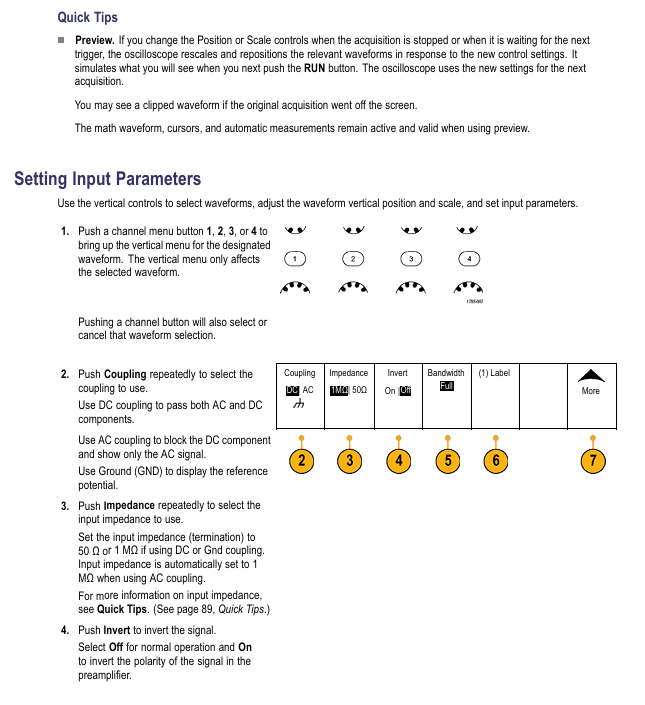
Coupling mode selection: Press the COUPLING button on CH1/CH2 to cycle through AC/DC/GND:
DC coupling: retaining the AC+DC components of the signal (such as measuring ripple with DC offset);
AC coupling: Block the DC component and only display the AC signal (such as measuring the amplitude of the AC signal);
GND coupling: Disconnect signal input and display ground reference line (used for calibrating vertical position);
ADD/MULT mode usage:
ADD mode: CH1 and CH2 signals are superimposed, and the CH1 VARIABLE knob can adjust the amplitude of CH2 signal to cancel interference (such as eliminating power noise);
MULT mode: The CH1 and CH2 signals are multiplied, and the result is automatically reduced by 5.12 times to adapt to the screen range (such as measuring power signals);
Bandwidth restriction application: When high-frequency noise interference occurs, press the BANDWIDTH button to select 20MHz/100MHz restriction to filter out high-frequency noise (such as selecting 20MHz bandwidth when measuring 50Hz power signals).
4.1.2 Common problem troubleshooting
No waveform display: Check if the coupling mode is GND → switch to AC/DC; Check if the probe is securely connected → Re plug and unplug the probe;
Waveform truncation: VOLTS/DIV sensitivity is too high → adjust clockwise to increase the gear;
High waveform noise: switch to AC coupling → enable bandwidth limitation → shorten the length of the probe ground wire.
4.2 Horizontal System (Signal Timing Control)
4.2.1 A/B dual time base operation
A time base (regular mode): Press the A button to activate, adjust the time base with SEC/DIV knob, and when ≤ 100ms/div, the AUTO trigger mode will automatically switch to ROLL mode (waveform scrolling display from left to right, suitable for slow signals);
B time base (delayed scan):
Press the B button to activate, and switch the SEC/DIV knob to control the B time base;
Adjust the A time base to display the complete signal, and adjust the B time base to amplify the signal locally (such as amplifying the rising edge of the pulse);
Press the A INTEN button, and the screen will display the A enhanced area (the local signal amplified by the B time base) for easy observation of details.
4.2.2 Trigger position adjustment
Press the TRIG POSITION button to cycle through the trigger positions (1/8, 1/4, 1/2, 3/4, 7/8):
Trigger position is 1/8: More display signals after triggering (such as observing the attenuation process after pulse triggering);
Trigger position is 7/8: more display of pre trigger signals (such as capturing interference pulses before triggering);
GPIB customization: Set non preset positions without screen underline identification through GPIB commands.
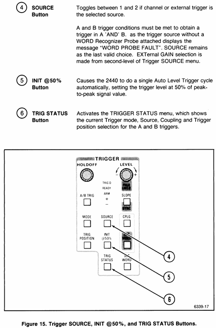
4.3 Trigger System (Stable Signal Display Core)
4.3.1 A/B Dual Trigger System Logic
A trigger is the “main trigger” (the initial condition for initiating data collection), and B trigger is the “delayed trigger” (further filtering of signals after the main trigger). It supports a combination of “main trigger+delayed event/time” trigger and is suitable for capturing signals with specific temporal relationships.
4.3.2 Detailed Explanation of Trigger Modes
Trigger Mode Function Description Applicable Scenarios
AUTO LEVEL automatically adjusts the trigger level to ensure stable display. Even when the signal disappears, regular signals (sine wave/square wave) can still be scanned for quick debugging
Stable triggering when the AUTO signal is present, and stopping scanning when the signal disappears requires clarification of the scene where the signal is present or absent
NORMAL is only triggered when the triggering conditions are met, and when there is no signal, the screen blank captures rare events (such as occasional pulses)
SINGLE SEQ single acquisition, automatically enters SAVE mode after completion to capture single transient signals (such as relay action)
4.3.3 Special triggering function (requires optional support)
Video trigger:
Press the SET Video button to enter the A Video COUPLING menu;
Select synchronization mode (Field 1/Field 2/ALT/TVLINE), only valid for interlaced signals;
Adjust TVLINE to select the trigger wire number, and CLAMP ON/OFF controls whether to clamp the synchronization signal;
Word trigger:
Press the SET WORD button to enter the Word Recognizer configuration menu;
Select encoding (OCT/HEX), clock signal (CLK), trigger word (such as 0x1234);
Only supports Word recognition probes, displaying “WORD PROBE FAULT” when there is no probe.
4.4 Delay function (capturing specific signals after triggering)
4.4.1 Delay by Events
Function: After A triggers, wait for a specified number of B triggering events before completing the collection;
Operation steps:
Press the DELAY → EVENT button to activate the event delay;
Rotate the CURSOR/DELAY knob to set the event count (such as 10, which is the 10th B event triggered for collection after A is triggered);
Press the TRIG STATION button and confirm that the trigger status is “ARMED”;
Applicable scenario: Capture the Nth data bit after the master clock in bus communication.
4.4.2 DELAY by TIME
Function: After triggering A, delay the specified time before completing the collection, supporting switching between “main delay” and “Δ delay”;
Operation steps:
Press the DELAY → TIME button to activate the time delay;
Rotate the CURSOR/DELAY knob to set the delay time (e.g. 100 μ s);
Press the Δ TIME button to switch to Δ delay mode and adjust the delay time increment;
Applicable scenario: Capture fault signals that occur after a delay in triggering (such as voltage attenuation after power is turned off).
4.5 Acquisition System (Signal Sampling and Processing)
4.5.1 Comparison of 5 acquisition modes
Working principle of collection mode, key parameters, applicable scenarios
Normal sampling, taking 1 sample point every interval – stable signal (sine wave/square wave), pursuing real-time performance
Average: After multiple acquisitions, take the average value to reduce random noise. The average number of times to reduce random noise is 2-256 for signals containing noise (power ripple, sensor output)
Envelope records the maximum/minimum sample points collected multiple times, generating envelope numbers: 1-256 times/CONT Observe the range of signal amplitude fluctuations (such as RF signal amplitude modulation)
Repet is only effective for repetitive waveforms, extending bandwidth to 300MHz – high-speed repetitive signals (clock signals, high-frequency pulses)
Save On Delta real-time comparison between live waveform and reference envelope, automatically stores reference memory when exceeding the limit: REF1-REF4 long-term monitoring occasional anomalies (such as ripple mutation, pulse distortion)
4.5.2 Acquisition mode switching and restart conditions
Switching method: Press the ACQUIRE button and select the mode and related parameters (such as average frequency and envelope frequency) from the menu;
Restart condition: The following actions will restart Average/Envelope collection:
Vertical/horizontal mode change;
Channel VOLTS/DIV or vertical position adjustment;
Press the SAVE button to enter the SAVEREF SOURCE menu;
Select storage source (such as CH1);
Enter the SAVEREF DESTIATION menu and select the storage target (REF1-REF4);
Confirm storage, the screen displays the prompt “STORED”;
Special function: Press the STACK REF button, and the waveform will be automatically stored in the preset order to REF1-REF4 (such as CH1 → REF1, CH2 → REF2).
4.6.2 Waveform Call (Display REF Button)
Calling steps:
Press the PLAY REF button to enter the PLAY REF menu;
Select the reference memory to be called (REF1-REF4), and display “EMPTY” when there is no waveform;
After calling, the horizontal position of the reference waveform can be adjusted according to HORIZ POS REF;
XY mode call: Select XYREF and call the XY combination waveform from REF1-REF4.
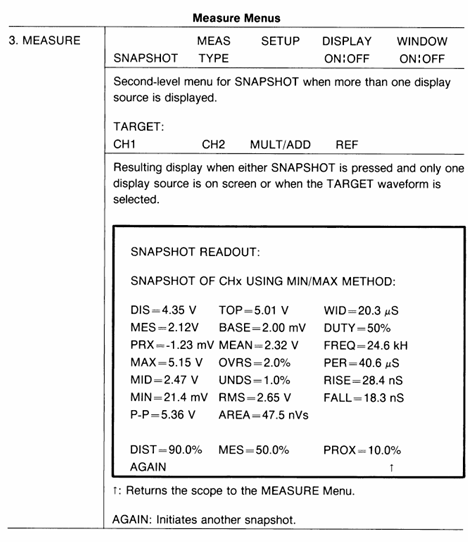
4.7 Measurement system (waveform parameter extraction)
4.7.1 Overview of Measurement Functions
Measurement type: 17 parameters, covering amplitude, time, and special categories:
Amplitude parameters: Peak to peak value (Pk Pk), maximum value (Max), minimum value (Min), mean (Mean), RMS, overshoot (Ovrsht), undershoot (Undrsht), area (Area);
Time parameters: Period, Freq, Rise, Fall, Width, Duty, Delay;
Special parameters: Events, Slope, 1/TIME (reciprocal frequency);
Measurement methods: continuous measurement (MEAS TYPE), single snapshot (SNAPSHOT).
4.7.2 Typical Measurement Operations (Taking “Rise Time” as an Example)
Preparation work: Ensure stable signal triggering, no obvious noise on the rising edge, and horizontal time base adaptation (such as measuring ns level rise time using 5ns/div);
Enter the measurement menu: press the Measure button;
Select measurement type: Press MEAS TYPE → check “RISE” in the parameter matrix;
Rotate the knob to adjust the levels of DISTAL (corresponding to 10%) and PROXIMAL (corresponding to 90%);
Press the MARK ON button, and the screen will display measurement markers (X-shaped) indicating the 10% and 90% level positions;
Reading result: The screen measurement reading area displays the rise time value (such as 28.4ns);
Single snapshot: Press SNAPSHOT → select the target channel (such as CH1), and the instrument captures all parameters of the current waveform and freezes the display.
4.8 GPIB Communication and Data Output (OUTPUT Button)
4.8.1 GPIB parameter configuration
Enter the configuration menu: press OUTPUT → SETUP;
Core parameter settings:
Mode: T/ONLY (only sends data), L/ONLY (only receives commands), T/L (sends and receives), DEVICES (connects to printer/plotter), OFF BUS (turns off GPIB);
Address (ADDR): Set GPIB address (such as 3) to match the controller address;
Terminator (TERM): EOI (default) LF/EOI, Ensure consistency with the receiving device;
Encoding (ENCDG): ASCII, RP (positive integer), RI (default), positive integer data should be set to RP;
Device adaptation: Press DEVICES → select device type (HPGL plotter, THINKJET printer) → set paper size (US: A4), whether to display scale (GRAT ON/OFF).
4.8.2 Data Transmission and Status Monitoring
Sending data: Press the TRANSMIT/RINT button to send the current waveform (CURVE), panel settings (PRGM), or measurement results to an external device;
Status monitoring: Press OUTPUT → STATUS to check the GPIB status (such as address, mode, error messages), with the undersigned item indicating the current effective setting;
Troubleshooting: If data transmission fails, check:
Is the GPIB cable connection secure;
Whether the address, terminator, and code are consistent with the receiving device;
Does the device support the selected data format (such as WHOLE WFMS/ARTIAL WFMS).
Safe operation and precautions
5.1 Safety prerequisites
It is necessary to refer to the “Operator Safety Summary” in the 2440 Operation Manual, with a focus on:
Input voltage limit: maximum 400Vpk for 1M Ω coupling, maximum 5Vrms for 50 Ω coupling;
Probe usage: Only use Tek recommended probes (such as 10X passive probes), and the probe ground wire must not be connected to mains power;
Grounding requirements: The instrument must be grounded through a 3-pin power supply and disconnection of the grounding pin is prohibited;
Do not use in damp or explosive environments, and do not plug or unplug probes or signal cables with power on.
5.2 Maintenance and Calibration
Signal Path Compensation (SPC): If the environmental temperature difference exceeds 10 ℃ or once a week, follow Utility → Calibration → Signal Path, which takes about 10 minutes to ensure low range (≤ 5mV/div) measurement accuracy;
Probe compensation: Every time the probe or channel is replaced, a CALIBRATOR circuit needs to be connected( 2.5V@1kHz )Adjust the compensation hole of the probe to a straight square wave;
Calibration prompt: If the extended diagnosis displays “UNCALD”, perform a SELF CAL after the instrument is preheated. If it still fails, contact a professional for calibration. At this time, the instrument may use the previous calibration parameters, and the measurement accuracy may decrease.
5.3 Common troubleshooting
Troubleshooting steps for possible causes of fault phenomena
No waveform display 1. Channel not activated; 2. The coupling method is GND; 3. Unstable triggering; 4. The brightness setting is too low. 1. Press MODE to activate the corresponding channel; 2. Switch the coupling to AC/DC; 3. Press AUTO SETUP or Initiat @ 50%; 4. Adjust the INTENSITY knob
Unstable triggering: 1. Improper triggering level; 2. The coupling method is not adapted; 3. Excessive signal noise. 1. Manually adjust TRIGGER LEVEL; 2. Enable Noise Reject coupling; 3. Switch to Average acquisition mode
Abnormal measurement result: 1. waveform truncation; 2. Inappropriate adaptation of time base/sensitivity; 3. Measurement standard error: 1. Adjust VOLTS/DIV to avoid waveform truncation; 2. Adapt to time base/sensitivity; 3. Adjust the measurement level by pressing MEASURE → SETUP
GPIB communication failure: 1. Address/code mismatch; 2. Cable malfunction; 3. Equipment not ready. 1. Check GPIB parameters; 2. Replace the cable; 3. Confirm that the external device is in a ready state
This manual is the official guidance document for the Tektronix MSO4000 (mixed signal) and DPO4000 (digital fluorescence) series oscilloscopes, covering 2-channel (such as MSO4032/DPO4032) and 4-channel (such as MSO4054/DPO4104) models, with a core focus on high-end electronic design and debugging (such as embedded systems, automotive electronics, communication equipment). The document structure includes 11 core chapters and 1 appendix, catering to the complex analysis needs of novice operators and professional engineers, highlighting the ability to synchronously collect and decode “analog+digital” mixed signals, as well as professional measurement functions extended through application modules.
Core parameters and characteristics of the product
1. Model classification and key parameters
Series models, analog channels, digital channels, bandwidth, maximum sampling rate, record length, typical applications
MSO4000 MSO4032 2 2 16 350MHz 2GS/s 10M point mixed signal debugging (such as I2C/SPI)
MSO4000 MSO4104 4 4 16 1GHz 5GS/s 10M high-speed signal capture (such as USB 2.0)
DPO4000 DPO4034 4-350MHz 2GS/s 10M point analog signal waveform analysis
DPO4000 DPO4104 4-1GHz 5GS/s 10M point high bandwidth signal (such as RF) testing
2. Core Features
Mixed signal analysis (MSO series exclusive): 16 digital channels and analog channels are synchronously collected, supporting MagniVu mode (60.6ps timing resolution), which can capture narrow pulses and edge jitter of digital signals;
High speed signal processing: The highest sampling rate for all channels is 5GS/s, with a recording length of 10M points. It supports a refresh rate of 50000 waveforms per second and can quickly capture transient anomalies;
Flexible triggering and decoding: 8 types of triggering types cover edge, pulse width, logic mode, and bus (such as I2C/CAN/RS-232), supporting sequence triggering (A event+delayed B event);
Professional Expansion Module: Extend functionality through modules such as DPO4PWR (Power Quality/Switching Loss Measurement) and DPO4USB (USB 2.0 Decoding) to meet vertical domain requirements;
Convenient data management: Supports CompactFlash, USB storage, Ethernet remote control (e * Scope), USBTMC protocol for direct connection to PC.
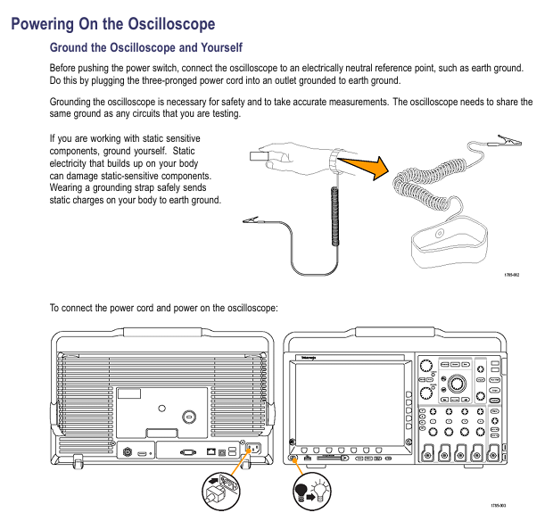
Grounding requirements: A 3-pin power cord must be used, and the equipment chassis must be reliably grounded. Floating operation is prohibited; During measurement, the reference end of the probe should only be connected to the signal ground and should not be connected to the mains ground.
2. Operation taboos
Do not use in damp (>90% RH) or explosive environments, and avoid liquid contact with equipment;
Before connecting/disconnecting the probe, the signal source must be disconnected first, and live plugging and unplugging are prohibited;
Before disassembling the application module or CF card, it is necessary to shut down and avoid short circuiting the battery or probe contacts.
Basic operation process
1. Probe operation and calibration
Key requirements for operation type steps
Passive probe compensation (P6139A) 1. Probe connected to CH1, set to 10X; 2. Connected to PROBE COMP( 2.5V@1kHz ); 3. Autoset; 4. Adjust the compensation hole to a flat square wave without overshoot/depression, and re compensate every time the channel is changed
Signal Path Compensation (SPC): 1. Disconnect all probes and preheat for 20 minutes; 2. Press 【 Utility 】 → 【 Calibration 】 → 【 Signal Path 】; 3. Wait for 10 minutes and display “Pass”. If the environmental temperature difference exceeds 10 ℃ or once a week, ensure low range (≤ 5mV/div) measurement accuracy
Firmware Upgrade 1. Download firmware. img from the official website to the USB root directory; 2. Turn off the oscilloscope and plug it into a USB port, and it will automatically upgrade when turned on; 3. After upgrading, verify the version (Utility ->Config ->About). During the upgrade, it is forbidden to power off or unplug the USB. It is recommended to use a blank USB to avoid file conflicts
2. Channel settings
Simulation channel:
Press the CH1-CH4 button to activate the channel, press 【 Coupling 】 to select DC/AC/GND (AC coupling blocks DC, GND displays reference ground);
Select 1M Ω/50 Ω (50 Ω only DC/GND coupling, maximum 1V/div) according to the ‘Impedance’ button;
Select Full/250MHz/20MHz (20MHz is used to filter out high-frequency noise) according to [Bandwidth];
Digital Channel (MSO Series):
Press 【 D15-D0 】 to activate the digital channel, and press 【 On/Off 】 to select D7-D0/D15-D8;
Set the threshold according to [Thresholds] (such as TTL 1.4V, 3.3V CMOS 1.65V);
Press MagniVu → On to enable 60.6ps timing resolution (for precise measurement of digital edges).
Core functional system
1. Collection system (5 modes)
The working principle of the collection mode is applicable to different scenarios
Peak Detect records the maximum/minimum value of each interval to capture narrow spikes (≥ 1ns), effective at low-speed time base (≥ 5 μ s/div)
Hi Res (High Resolution) calculates the average value of each interval sample to reduce noise and improve the resolution of low-frequency signals
Envelope records the maximum/minimum waveform collected multiple times, observing the range of signal amplitude changes (such as power ripple fluctuations)
Average: After multiple acquisitions, the average (4/16/64/128 optional) suppresses random noise, and averaging 128 times can significantly improve the signal-to-noise ratio
2. Trigger system (8 types)
Trigger type key parameters applicable scenarios
Edge slope (rising/falling), coupling (DC/LF Reject/HF Reject), stable display of conventional signals (such as clock, square wave)
Pulse Width condition (>/</=/≠), width (33ns-10s), polarity capture of abnormal pulses (such as narrow pulse interference in communication links)
Logic channel status (High/Low/Don’t Care), clock edge multi-channel logic combination triggering (such as I2C SDA=1 and SCL=0)
Setup&Hold: Clock channel, data channel, violation time detection bus timing violation (such as insufficient setup time between FPGA and memory)
Bus type (I2C/CAN/RS-32, etc.), trigger conditions (address/data/error), decode and trigger bus specific events (such as Write operation for I2C address 0x7F)
3. Measurement and analysis functions
Automatic measurement: Supports 11 types of parameters, with a maximum of 8 displayed simultaneously. The key measurements are as follows:
Measurement type definition accuracy conditions
The amplitude of the reciprocal signal of the first cycle of frequency (Freq) is ≥ 1div, without any truncation
Rise Time: The time signal with an amplitude of 10% -90% has no noise on the rising edge and is horizontally scale adapted (such as 10ns/div)
Peak to peak value (Pk Pk) full waveform maximum minimum value waveform without truncation, vertical scale adaptation (such as 100mV/div)
FFT spectrum analysis:
Press 【 Math 】 → 【 FFT 】, select the source channel (such as CH1);
Press [Window] to select the window function (Rectangular: optimal frequency resolution; Blackman Harris: excellent amplitude accuracy);
Select dBV RMS/Linear RMS according to ‘Vertical Units’ (dBV RMS is suitable for multi frequency comparison);
Connect the Ethernet cable to the rear panel LAN port, press 【 Utility 】 → 【 I/O 】 → 【 Ethernet Network Settings 】;
Set DHCP to On (automatically obtain IP) or Off (manually set IP);
Input the oscilloscope IP into the PC browser and access the e * Scope interface to control the oscilloscope;
USBTMC (PC Control):
Connect the Rear panel USB Device port of the oscilloscope to the PC using a USB cable;
Install VISA driver (official website download), and send SCPI command through LabVIEW/Excel on the PC end;
Application modules and case studies
1. Optional application modules
Module model, function, applicable scenarios
DPO4PWR power analysis: power quality, switching losses, harmonics, safe working area (SOA) power supply design (such as AC-DC converter efficiency testing)
DPO4USB 2.0 decoding: low-speed/full speed bus triggering and decoding, supporting PID error detection and USB device debugging (such as troubleshooting USB disk enumeration failures)
DPO4AUTO Automotive Bus: CAN/LIN triggering and decoding, supporting frame type/ID filtering for automotive electronics (such as CAN bus communication faults)
DPO4VID video trigger: HDTV (such as 1080i), custom video (3-4000 lines), video equipment (such as monitoring camera signal testing)
2. Typical troubleshooting cases
Case 1: Abnormal RS-232 bus
Connection: CH1 is connected to the TX line, CH2 is connected to the RX line, press 【 B1 】 → 【 Bus 】 → 【 RS-232 】;
Set parameters: baud rate 9600, data bit 8, parity None, stop bit 1;
Trigger: Press 【 Trigger Menu 】→【 Type 】→【 Bus 】→【 Trigger On 】→【 Tx Data 】, set the trigger data to 0x55;
Analysis: Press 【 Search 】 → 【 Bus 】 → 【 Tx Data 】, mark all 0x55 frames, and use Wave Inspector to view the timing of abnormal frames;
Case 2: Relay arc capture
Parameter setting: CH1 is connected to both ends of the relay, Vertical scale 100V/div,Horizontal scale 10μs/div;
Trigger: Press 【 Trigger Menu 】→【 Type 】→【 Edge 】→【 Slope 】→【 Rising 】, set the trigger level to 50V;
Capture: Press [Single] to trigger when the relay is disconnected, observe the peak generated by the arc (amplitude>200V);
Optimization: Zoom in on the peak area (Zoom x 10) and measure the peak width with the cursor (approximately 50ns).
Appendix and Support
1. Key performance parameters
System parameter description
Analog channel DC gain accuracy ± 1.5% (1M Ω path), ± 3% (50 Ω path), with a 0.1% decrease per ℃ above 30 ℃
The timing resolution of the digital channel (MSO) is typically 121ps, while in MagniVu mode it is 60.6ps
Trigger system edge trigger sensitivity DC coupling: 1div (DC-10MHz), 2div (100-1GHz)
Display system screen resolution 1024 × 768 pixels (10.4-inch XGA)
2. Probe compatibility
Probe model, type, bandwidth, maximum voltage, applicable scenarios
P6139A (standard) passive voltage 500MHz CAT II 300V RMS conventional analog signal measurement
P6516 (MSO standard) logic probe DC-100MHz ± 15V digital channel signal acquisition
TCP303 (optional) current probe DC-15MHz 150A RMS high current AC/DC measurement
P5200 (optional) differential probe DC-200MHz 1000V RMS high-voltage differential signal (such as motor drive)
The official guide document for the Tektronix TPS2000 series digital storage oscilloscope covers the 2-channel (TPS2012) and 4-channel (TPS2014/TPS2024) models, with a core positioning for portable isolation measurement scenarios (such as industrial equipment floating ground testing and outdoor on-site maintenance). The document structure is clear, gradually deepening from safety specifications to advanced functions, including 11 core chapters and 6 appendices, catering to both novice operation and professional measurement needs, while providing rich diagrams and step instructions to reduce operational complexity.
Core parameters and characteristics of the product
1. Model classification and key parameters
Model Number of Channels Bandwidth Sampling Rate Single Battery Endurance Dual Battery Endurance
TPS 2012 2 100MHz 1GS/s 5.5 hours 11 hours
TPS 2014 4 100MHz 1GS/s 4.5 hours 9 hours
TPS2024 4 200MHz 2GS/s 4.5 hours 9 hours
2. Core Features
Isolation channel: All channels and Ext Trig inputs are isolated from chassis, supporting independent floating ground measurement with an input impedance of 3M Ω, solving the common ground limitation of traditional oscilloscopes;
Portable power supply: compatible with TPSBAT lithium batteries (standard 1, optional 2), can be charged simultaneously when powered by mains electricity;
Full function analysis: supports peak detection (capturing ≥ 10ns glitches), video triggering (NTSC/PAL/SECAM), FFT spectrum analysis (2048 point transform);
Data interface: Front mounted Type 1 CompactFlash card slot, rear mounted RS-232 (9-pin) and Centronics (parallel printing) interfaces.
Safety operation standards
1. Electrical safety
Voltage limitation: The maximum voltage of the input channel is 300V RMS CAT II. When it exceeds 100kHz, it will attenuate by 20dB/tenfold to avoid arc damage;
Probe safety: The reference end of the P2220 probe is prohibited from floating above 30V RMS. For high voltage measurements, P5120 (600V RMS CAT II) or differential probes are required;
Grounding requirements: A 3-pin power cord must be used and disconnection of the grounding is prohibited; The equipment chassis needs to be reliably grounded to avoid electric shock caused by floating operations.
2. Operation taboos
Prohibit use in damp/explosive environments and avoid liquid spraying equipment;
Before connecting/disconnecting the probe, the signal source must be disconnected first, and live operation is prohibited;
Before disassembling the battery, it is necessary to turn off the device and avoid short circuiting the battery contacts or putting them into a fire.
Basic operation process
1. Probe operation
Key requirements for operation type steps
Manual compensation: 1. Connect the probe to CH1 and set it to 10X; 2. Connect it to PROBE COMP; 3. Autoset; 4. Adjust the compensation hole to a square wave that is flat and free of dents/bulges. Re compensate each time the channel is changed
Attenuation setting 1. Press CHx MENU → Probe → Voltage Attenuation; 2. Choose 1X/10X P2220 and set the bandwidth limit to 6MHz for 1X
Current probe scaling 1. Press CHx MENU → Probe → Current → Scale; 2. Choose a matching value (such as 10A/V) to ensure consistency with the output ratio of the current probe and avoid reading deviation
2. Self calibration and firmware updates
Self calibration:
Disconnect all probes and press 【 Utility 】 → 【 Do Self Cal 】;
Wait for 2 minutes, and upon completion, display ‘Calibration PASSED’;
Trigger condition: If the environmental temperature difference exceeds 5 ℃ or once a week, preheating for 20 minutes is required.
Firmware update:
Download the latest firmware from the official website and copy it to the root directory of CompactFlash;
Insert the oscilloscope and press 【 Utility 】 → 【 File Utilities 】 → 【 Update Firmware 】;
Wait for completion, do not power off or unplug the card.
Core Systems and Functions
1. Collection system (three modes)
The working principle of the collection mode is applicable to different scenarios
Peak detection mode records the maximum/minimum values of each interval, including signals with spikes and narrow pulses (≥ 10ns)
After multiple acquisitions in average mode, the signal containing random noise (power ripple, sensor output) is averaged (4/16/64/128 times)
2. Trigger system (three types)
Trigger type key parameters applicable scenarios
Edge triggered slope (rising/falling), coupling (AC/DC/noise suppression), stable display of conventional signals (such as clock signals)
Video trigger standards (NTSC/PAL/SECAM), synchronous (field/line) composite video signals (such as medical equipment video output)
Pulse width triggering condition (=≠<>), width (33ns-10s), polarity capture abnormal pulse (such as communication link narrow pulse interference)
3. FFT spectrum analysis
Setting steps:
Center the time-domain signal (align the 0V line with the center of the screen) to ensure complete waveform;
Press Math Menu → Operation → FFT to select the source channel;
Window selection function (Hanning window: excellent frequency resolution; flat top window: excellent amplitude accuracy).
De aliasing method:
Increase sampling rate (switch from SEC/DIV to faster gear);
Enable 20MHz bandwidth limit;
External filtering (adding a low-pass filter at the signal source end).
Battery Management (Core Features)
1. Charging and battery life
Charging method: single battery charging time, dual battery charging sequence, battery life (4-channel model)
In machine (power on), charge the high battery first for 7 hours, then charge the low battery for 4.5 hours (single battery), and 9 hours (dual battery)
In machine (standby) 4.5 hours as above-
External TPSCHG charger can charge 2 units simultaneously in 3 hours-
2. Calibration and maintenance
Calibration:
External calibration: TPSCHG charger left slot → press “Recalibrate”, takes about 10 hours (charge discharge cycle);
In machine calibration: discharge to shutdown → charge for 5 hours → discharge to shutdown → recharge for another 5 hours.
Storage:
Temperature: 5-20 ℃, humidity ≤ 80%;
Electricity consumption: about 50%, replenished once every 6 months;
Taboo: Long term full charge (>80%) or empty charge (<20%) storage is prohibited.
Data Storage and Communication
1. CompactFlash card operation
Storage Content File Name Format 1MB Capacity Approximately Storage Quantity Key Operations
Set file FnnnnTEK.SET to 250, press 【 Save/Recall 】 → 【 Save Setup 】 → select storage location
16 image files FnnnnTEK.BMP, press [Print] (set to “Save Image to File”)
2. RS-232 communication settings
Parameter configuration: Press 【 Utility 】 → 【 Options 】 → 【 RS232 Setup 】 to set the baud rate (default 9600), flow control (Hardtagging), and checksum (None);
Test steps:
Connect the oscilloscope to the PC using cable 012-1379-00;
Open HyperTerminal on the PC and set the same parameters;
Send ‘ID?’, the oscilloscope returns’ ID TEK/TPS2024, CF: 91.1CT, FV: V10.00 ‘.
Typical application cases
1. Isolation channel measurement differential signal
Connect the probe tip to the positive terminal of the differential signal and the reference terminal to the negative terminal (no common ground required);
Press’ AutoSet ‘to display the differential waveform;
Press’ Single Seq ‘to capture a snapshot, and use the cursor to measure the amplitude/rise time.
2. Video signal triggering (NTSC)
Connect the probe to video output, press 【 CH1 MENU 】 → 【 Coupling 】 → 【 AC 】;
Press 【 Trig Menu 】→【 Type 】→【 Video 】→【 Standard 】→【 NTSC 】;
Select [Sync] → [All Lines], adjust SEC/DIV to 500ns/div, and observe the color synchronization signal.
3. Power waveform measurement (voltage x current)
CH1 connected to voltage probe (10X), CH2 connected to current probe (10A/V);
Press 【 Math Menu 】→【 Operation 】→【 × 】→【 CH1 × CH2 】;
Adjust the Math waveform position/scale to display instantaneous power (in VA).
Appendix and Support
1. Key performance parameters
System parameter description
Vertical system resolution 8-bit, 2mV-5V/div
Horizontal system time base range TPS2024:2.5ns-50s/div; TPS2012/2014:5ns-50s/div
Trigger system edge trigger sensitivity DC coupling: 1div (DC-10MHz), 2div (100-200MHz)
Display system resolution of 320 × 240 pixels, 5.7-inch LCD
2. Probe compatibility
Probe model, attenuation ratio, bandwidth, maximum voltage, applicable scenarios
P2220 (Standard) 1X/10X 6MHz/200MHz 150V/300V RMS CAT II Conventional Voltage Measurement
P5120 (optional) 20X 200MHz 1000V RMS CAT II high voltage measurement
TCP303 (optional) 5/50mV/A 15MHz 150A RMS high current AC/DC measurement
This manual is the official guidance document for the Tektronix TBS1000B (General Edition) and TBS1000B-EDU (Education Edition) series of digital storage oscilloscopes, covering the entire process of product safety operation to advanced functional applications. It is suitable for engineers, technicians, and teachers and students in educational settings. The manual has a clear structure and includes modules such as safety information, basic operations, core functions, application cases, performance parameters, and probe information. At the same time, through tables, diagrams, and step-by-step instructions, it reduces operational complexity and ensures that users can quickly master the use and maintenance of the oscilloscope.
Product model and core parameters
1. Model classification and key parameters
Applicable scenarios for model bandwidth sampling rate
TBS1032B 30MHz 500MS/s Basic Low Frequency Measurement (North America/Europe only)
TBS1052B/TBS1052B-EDU 50MHz 1GS/s Universal Low Frequency Testing and Educational Experiment
Analysis of Low Frequency Signals in TBS1072B/TBS1072B-EDU 70MHz 1GS/s
TBS1102B/TBS1102B-EDU 100MHz 2GS/s High Frequency Digital Signal Test
TBS1152B/TBS1152B-EDU 150MHz 2GS/s High Speed Serial Signal Analysis
TBS1202B/TBS1202B-EDU 200MHz 2GS/s ultra high speed signal (such as DDR memory) testing
2. General core features
Channel configuration: 2 analog channels, supporting simultaneous measurement of 2 signals
Record length: fixed 2500 points/channel to ensure complete signal details
Display screen: 7-inch color LCD, supporting vector/dot display mode
Storage interface: front USB flash drive port (supporting ≤ 64GB), rear USB device port (connected to PC/GPIB)
Language support: 11 languages (including Chinese, English, Japanese, Korean, Russian, etc.)
Safety operation standards
1. Electrical safety
Grounding requirements: A 3-pin power cord must be used, and the grounding conductor must be connected to the ground. It is forbidden to disconnect the grounding
Voltage limitation: The maximum voltage of the input channel is 300V RMS CAT II, and when it exceeds 100kHz, it attenuates by 20dB/tenfold
Probe safety: When using TPP series probes, fingers should be placed behind a protective barrier and touching the metal parts of the probe is prohibited
2. Operation taboos
Prohibited from use in damp/explosive environments, avoid liquid spraying equipment
It is prohibited to dismantle the equipment casing as high internal voltage may cause electric shock
When connecting/disconnecting the probe, the signal source should be disconnected first to avoid arc damage
Basic operation process
1. Equipment installation and functional inspection
Power connection: Connect to a 90-264VAC/45-66Hz power supply, with a maximum power consumption of 30W
Secure fixation: Fix equipment through safety lock holes or cable channels to prevent slipping
Functional check:
Press’ Default Setup ‘to restore factory settings
Connect the probe to CH1, and connect the probe tip to the PROBE COMP terminal( 5V@1kHz Square wave
Press [Autoset], the screen should display a stable square wave, and the calibration status should be “PASSED”
2. Probe operation
Manual compensation:
Probe connected to CH1, set attenuation to 10X
Connect the probe tip to [PROBE COMP] and press [Autoset]
Adjust the probe compensation hole to make the square wave edge straight (to avoid overcompensation/undercompensation)
Attenuation setting: default 10X, P2220 probe supports 1X/10X switching (bandwidth limited to 6MHz at 1X)
Current probe: The scaling ratio needs to be manually set (default 10A/V) to ensure accurate readings
3. Self calibration and firmware updates
Self calibration:
Trigger condition: If the environmental temperature difference exceeds 5 ℃ or once a week, preheating for 20 minutes is required
Operation steps: Disconnect all probes → 【 Utility 】 → 【 Do Self Cal 】 → Follow the prompts to complete (about 2 minutes)
Firmware update:
Download the latest firmware from the official website (www.tektronix. com/software)
Copy to the root directory of the USB flash drive and insert the oscilloscope
Auto: Automatically scans without triggering, suitable for signal exploration
Normal: Only displayed when triggered, suitable for stable signal observation
Single: Single capture, suitable for transient signals (such as relay arcs)
4. Acquisition Controls
The working principle of the collection mode is applicable to different scenarios
Sampling mode equidistant sampling, 1 sampling point=1 waveform point for most conventional signals
Peak detection mode records the maximum/minimum values within each interval, captures narrow pulses (≥ 10ns), and reduces aliasing
After multiple acquisitions in average mode (4/16/64/128 times optional), suppress random noise and improve signal clarity
Measurement and analysis functions
1. Basic measurement techniques
Voltage measurement:
Peak to Peak Value (Vp-p): The difference between the maximum and minimum values of the signal, calculated by multiplying the number of vertical partitions by volts per grid and the probe attenuation ratio
Amplitude: Voltage from ground to signal peak, for example: 2V/div x 3 zones x 10X probe=60V
Time measurement:
Cycle/frequency: Cycle=number of horizontal partitions x seconds/grid, frequency=1/cycle
Pulse width: time interval at 50% amplitude, rise/fall time: time interval at 10% -90% amplitude
Phase difference measurement: Turn on XY mode and use the Lissajous diagram to determine (for example, when the frequency ratio is 1:1, the straight line is 0 ° and the circle is 90 °)
2. Automatic measurement and FFT analysis
Automatic measurement:
Supports 34 types, including time class (cycle, frequency, delay), amplitude class (peak to peak, overshoot), and count class (pulse number, edge number)
Up to 6 measurement results can be displayed simultaneously, with an update frequency of approximately 2 times per second
FFT analysis:
Window function selection: Hanning window (excellent frequency resolution), flat top window (excellent amplitude accuracy), rectangular window (transient analysis)
Nyquist frequency: half of the sampling rate. Exceeding this frequency will result in aliasing, which needs to be resolved by increasing the sampling rate or filtering
Spectrum measurement: supports cursor measurement of frequency (Hz) and amplitude (dB, 0dB=1VRMS)
Data storage and transmission
1. USB flash drive operation
Storage content and capacity (approximately per 1MB):
250 setup files (. SET)
18 waveform files (. CSV, containing 2500 point time amplitude data)
Environmental adaptability: Working temperature 0-50 ℃, humidity ≤ 85% (below 40 ℃)
2. Probe information (TPP series)
Model bandwidth attenuation ratio compensation range, maximum input voltage
TPP0051 50MHz 10:1 15-25pF 300V RMS CAT II
TPP0101 100MHz 10:1 15-25pF 300V RMS CAT II
TPP0201 200MHz 10:1 15-25pF 300V RMS CAT II
3. Equipment maintenance
Cleaning: Use a lint free cloth dipped in 75% isopropanol to wipe the outer shell, avoiding the use of abrasion cleaner
Calibration: It is recommended to conduct factory calibration annually and contact the Tech service center
Troubleshooting: Check the error log through 【 Utility 】 → 【 System Status 】. Common issues include probe not compensating and improper trigger settings
The XYZs of Oscilloscopes Primer launched by Tektronix aims to help engineers, technicians, educators, and others master the basic knowledge and operation of oscilloscopes, without the need for prior mathematical or electronic knowledge. Through theoretical explanations, chart examples, exercises, and terminology lists, it covers the entire process of oscilloscopes from principle to practice, ultimately allowing readers to describe the working principle of oscilloscopes, distinguish oscilloscope types, understand waveforms and controls, and complete basic measurements.
Signal Integrity
Core significance: The ability of oscilloscope systems to accurately reconstruct waveforms, analogous to the “imaging accuracy” and “clarity” of cameras, directly affects the time to market cycle of electronic design, product reliability, EMI compliance, and probe can also affect the signal integrity of measurement systems.
Root cause of the problem:
Speed improvement: The processor clock speed reaches 2-5GS/s, the DDR3 memory clock exceeds 2GHz, the rise time is 35ps, and the high-speed characteristics penetrate into fields such as automotive and consumer electronics, with most designs becoming “high-speed designs”.
Physical limitations: The propagation time of the circuit board bus has remained unchanged for decades, and 6-inch traces become transmission lines when the signal rise time is less than 4-6ns, causing crosstalk, ground bounce, and EMI rise.
Model failure: When the signal edge velocity is 4-6 times or more the signal path delay, the lumped circuit model is no longer applicable.
Solution: Digital errors often stem from simulation problems, and it is necessary to use an oscilloscope to observe waveform details, transient signals, and correlate high-speed waveforms with data patterns.
Principle and waveform of oscilloscope (The Oscilloscope)
(1) Working principle
Oscilloscope is a graphical display device that converts electrical signals into a “time voltage” graph
X-axis (horizontal): Time
Y-axis (vertical): voltage
Z-axis (brightness): Display intensity (represented by color grading in DPO to indicate signal frequency)
(2) Waveform types and characteristics
Application scenarios of key characteristics of waveform types
Sine wave mathematical harmony, AC power supply, signal generator output basic test signal, power supply voltage
Square wave/rectangular wave square wave high and low level time are equal, rectangular wave unequal amplifier testing, timing signal (TV/computer)
Linear variation of sawtooth/triangular wave voltage (ramp) simulation oscilloscope horizontal scanning, TV grating scanning
Step/pulse step is a sudden voltage change, pulse is an “on-off” change power switch, computer data transmission (1-bit information), radar
Periodic/non periodic periodic periodic signal repetition, non periodic signal continuous change periodicity: sine wave; Non periodic: transient faults
Synchronous/asynchronous synchronous signals have a timing relationship (such as clock and data), asynchronous signals have no (such as keyboard and computer clock). Synchronization: internal signals of the computer; Asynchronous: Peripheral interaction
Complex waves combined with multiple waveform features, including amplitude/phase/frequency variation composite video signals and communication eye diagrams (such as 622Mb/s serial data)
(3) Waveform measurement indicators
Frequency and Period: Frequency (Hz)=1/Period (seconds), for example: A 3Hz sine wave has a period of 1/3 second.
Voltage: Peak to Peak Value (Vp-p, signal maximum to minimum voltage difference), Peak Value (Vp, ground to maximum voltage).
Amplitude: usually refers to the maximum voltage from ground to the signal. For example, a waveform with an amplitude of 1V has a peak to peak value of 2V.
Phase: Sine wave 1 cycle=360 °, phase difference refers to the timing difference between two similar signals, for example: current and voltage differ by 90 ° (1/4 cycle).
Automatic measurement of digital oscilloscope: including cycle, duty cycle, frequency, delay, maximum/minimum value, rise/fall time, overshoot RMS、 Shake, etc.
Types of Oscilloscopes
Type Core Architecture Key Features Applicable Scenarios
Digital Storage Oscilloscope (DSO) serial processing (amplification → ADC → storage → microprocessor → display) stores transient signals, permanently saves and processes them, without real-time brightness grading, low-speed repetition or single high-speed multi-channel design (such as capturing glitches)
Digital Fluorescence Oscilloscope (DPO) parallel processing (amplification → ADC → digital fluorescence database → direct display, microprocessor parallel processing) real-time 3D display (time, amplitude, amplitude distribution), high waveform capture rate (million level/second), general design and troubleshooting of analog oscilloscope display characteristics (video signal, communication mask testing)
Mixed domain oscilloscope (MDO) combined with RF spectrum analyzer+MSO/DPO to correlate digital, analog, and RF signal time, reducing measurement uncertainty of cross domain events. Embedded RF design (such as Zigbee radio, observing command and RF event delay)
Mixed signal oscilloscope (MSO) combined with DPO performance and 16 channel logic analyzer to simultaneously observe analog and digital signals, supporting protocol decoding (I2C/CAN, etc.) and digital circuit debugging (verifying the correlation between logic state and analog waveform)
Digital sampling oscilloscope first samples and then amplifies (sampling bridge → amplification) with high bandwidth (up to 80GHz), limited dynamic range (1Vp-p), safe input voltage of 3V, measurement frequency exceeding the oscilloscope sampling rate for repetitive signals (such as high-speed timing)
Oscilloscope Systems and Controls
(1) Vertical System and Control
Core functions: Adjust the vertical position and scaling of waveforms, set signal coupling and bandwidth.
Key controls:
Position and volts/div: volts/div is the scaling factor, for example: 5V/div x 8 vertical partition=40V maximum display voltage; Combined with probe attenuation (10X probe needs to be divided by 10).
Input coupling: DC (display full signal), AC (block DC, center signal), GND (disconnect input, display 0V line).
Bandwidth limitation/enhancement: Bandwidth limitation reduces noise, while bandwidth enhancement (DSP filtering) expands bandwidth and improves phase linearity.
(2) Horizontal System and Control
Core function: Control signal acquisition (sampling mode, sampling rate) and waveform horizontal position, scaling.
Key controls and concepts:
Sampling mode:
Sampling mode: 1 sampling point=1 waveform point.
Peak detection mode: Save the maximum/minimum values within 2 waveform intervals to capture fast transients (such as narrow pulses).
High resolution (Hi Res) mode: averaging multiple sampling points to reduce noise, suitable for a single event.
Envelope mode: displays the range of signal variation based on the maximum/minimum values collected multiple times.
Average mode: Average the waveform points collected multiple times, reduce noise, and repeat the signal.
Sampling method:
Real time sampling: Collect enough points in one scan, suitable for signals with a frequency<1/2 of the oscilloscope’s maximum sampling rate, and the only method to capture a single transient.
Equivalent time sampling: Multiple scans capture repeated signal segments (random: sampling clock is asynchronous with trigger, supports pre trigger; sequential: delay increment Δ t per trigger, high time resolution), suitable for frequency oversampling rate of repeated signals.
Position and Sec/div: Sec/div is the time base, for example: 1ms/div x 10 horizontal partitions=10ms total display time.
Other: Time base selection (main time base/delay time base), scaling/shifting, searching (finding specific events), XY mode (X-axis is the signal rather than time, measuring phase difference).
(3) Trigger system and control
Core function: Synchronize horizontal scanning, stabilize repetitive waveforms or capture single waveforms.
Key controls and types:
Trigger position: The digital oscilloscope supports pre triggering (observing events before triggering), while the analog oscilloscope does not (except for a few delay lines).
Trigger level and slope: The level is the trigger voltage threshold, and the slope is the rising edge (positive) or falling edge (negative).
Trigger mode: Normal mode (scanning only when the signal reaches the threshold, black screen/freeze when there is no signal), Automatic mode (timer triggered when there is no trigger, ensuring display).
Trigger coupling: AC/DC/GND, and high-frequency/low-frequency/noise suppression (reducing false triggering).
Trigger suppression: After triggering, there is a “blind period” to avoid accidentally triggering complex waveforms.
Advanced triggers: burr trigger (capturing pulse width exceeding limit), pulse width trigger (capturing pulse width exceeding limit), establish hold time trigger (capturing timing violations), serial/parallel protocol trigger (such as I2C/CAN, parallel bus), etc.
(4) Display system and other controls
Display system: scale lines (8 × 10 or 10 × 10 partitions, including primary and secondary partitions), displaying volts/div and sec/div parameters.
Other controls: mathematical operations (addition, subtraction, multiplication, division, integration, FFT), digital timing and state acquisition (MSO digital channel, timing acquisition: fixed sampling rate; Status collection: clock definition of valid status.
Complete Measurement Systems (Probes)
(1) Probe type and characteristics
Probe type, core characteristics, and precautions
Passive probe universal, low cost, 10X attenuation reduces circuit load, 1X no attenuation 10X probe requires compensation (balance probe and oscilloscope electrical characteristics); 1X is susceptible to interference and suitable for low-speed, low amplitude signals
Active and differential probes contain dedicated ICs, high fidelity, low load, suitable for high speed (such as LVDS), and differential signals require DC power supply (some through oscilloscope interfaces); Can simultaneously measure differential, single ended, and common mode signals
Logic probe MSO specific, 2 8-channel pods, rechecked grounded, low capacitance load (reduces signal distortion), blue coaxial labeled first channel, universal grounding compatible with custom connections
Specialized probes for current, high voltage, optical probes, etc., converting non electrical signals into electrical signals requires matching the measurement scenario (such as high voltage probes for measuring voltage signals)
(2) Probe accessories and selection
Intelligent interface: Automatically identify probe attenuation (such as 10X) and type, adjust oscilloscope display.
Grounding lead adapter: Shortens the grounding distance from the probe tip to the DUT, improving high-speed signal integrity.
Selection principle: Probe+oscilloscope bandwidth ≥ signal maximum frequency × 5, minimize load (resistance/capacitance/inductance).
Performance Terms and Considerations
(1) Core performance parameters
Parameter definition and key data calculation formula/rule
The bandwidth sine signal attenuates to a frequency of 70.7% (-3dB), which determines the high-frequency response of the signal by 5 times. The rule is: oscilloscope bandwidth ≥ signal highest frequency component × 5
The rise time of the signal from 10% to 90% amplitude reflects the ability to capture rapid changes by 1/5 rule: oscilloscope rise time ≤ fastest rise time of the signal × 1/5; Rise time=k/bandwidth (k=0.35-0.45, 0.35 for<1GHz, 0.40-0.45 for>1GHz)
Sampling rate per second (S/s) determines real-time sampling of waveform details: sinx/x interpolation must be ≥ 2.5 times the highest frequency of the signal; Linear interpolation requires ≥ 10 times the highest frequency of the signal
The waveform capture rate is the number of waveforms captured per second (wfms/s), which determines the transient event capture probability DPO: in the millions per second; DSO: Level 10-5000 per second
Record the number of sampling points for a single waveform to determine the data volume. Time interval=record length/sampling rate, for example: 100k point record length, 1GS/s sampling rate, time interval=100 μ s
The effective number of bits measures the accuracy of ADC reconstruction of sine waves, and the signal frequency and amplitude need to be specified for noise and distortion effects
The ability of a vertical amplifier to amplify weak signals with vertical sensitivity, measured in mV/partition. The minimum voltage for a general-purpose oscilloscope is approximately 1mV/partition
The accuracy of timing displayed by the time base precision level system is usually a percentage error (such as ± 0.01%)
(2) Other considerations
Scalability: Supports increasing memory, application modules (such as jitter analysis, video testing), and third-party software (MATLAB).
Usability: Front panel partition (vertical/horizontal/triggered), graphical interface, touch screen, portability (suitable for laboratory/field).
Oscilloscope Operation&Measurement Techniques
(1) Operation steps
Correct grounding:
Oscilloscope: 3-pin power plug grounded to prevent electric shock and ensure measurement reference.
Personnel: Wear a grounding wristband when in contact with IC to prevent static damage (IC conductive path is fragile).
Control settings:
Vertical: Select the channel, center the voltage/grid and position, couple with DC, and turn off the variable gain.
Horizontal: seconds/grid and centered position, record length can be selected as needed.
Trigger: Set the mode to automatic, select the current channel as the source, center the trigger level, and set the minimum suppression.
Calibration: If the ambient temperature changes by more than 5 ℃ or once a week, perform “signal path compensation” (refer to oscilloscope manual).
Probe connection and compensation:
Connection: Connect the probe tip to the test point and the grounding clip to the DUT ground (such as metal chassis).
Compensation: Connect the probe to the oscilloscope square wave reference signal and adjust the probe to make the square wave edge straight (to avoid measurement errors caused by under/over compensation).
(2) Measurement technology
Voltage measurement:
Adjust the voltage/grid to make the signal occupy 80% of the vertical partition (improve accuracy).
Number signal vertical span (number of partitions), voltage=number of partitions x volts/grid x probe attenuation ratio (e.g. 10X).
Example: 2V/div, signal occupying 4 zones, 10X probe, voltage=4 × 2V × 10=80V (peak to peak).
Time and frequency measurement:
Adjust the seconds/grids to ensure that the signal cycle occupies the full horizontal partition.
The horizontal span of the signal period (number of partitions), period=number of partitions x seconds/grid; Frequency=1/cycle.
Example: 1ms/div, period occupies 5 partitions, period=5 × 1ms=5ms, frequency=1/5ms=200Hz.
Pulse width and rise time measurement:
Pulse width: Measure the horizontal span at 50% amplitude of the signal, multiplied by seconds per grid.
Rise time: Measure the horizontal span at 10% -90% amplitude of the signal, multiplied by seconds per grid.
Phase difference measurement:
Turn on XY mode, CH1 is connected to signal 1 (Y-axis), CH2 is connected to signal 2 (X-axis), forming a Lissajous pattern.
Determine the phase difference based on the shape of the graph (e.g. 1:1 frequency ratio, 0 ° for straight lines, 90 ° for circles).